Avishek Sarbajna, Dorte Rubæk Danielsen, Laura Nevenka Casses, Nicolas Stenger, Peter Bøggild, Søren Raza
Encapsulated Void Resonators in Van der Waals Heterostructures
Laser & Photonics Reviews, Early View Online Version of Record before inclusion in an issue 2401215
DOI: https://doi.org/10.1002/lpor.202401215
Min Liu, Tobias Reimer, Yongkang Wang, Mathias Kläui, Yaowen Xing, Xiahui Gui, Yijun Cao, Rüdiger Berger, Hai Wang and Mischa Bonn
Mechanically Stable PMMA-Based Large-Area Nano-Channels with Sub-10 nm Depth
Advanced Materials Technologies, Online Version of Record before inclusion in an issue, 2401172
DOI: https://doi.org/10.1002/admt.202401172
Liu, Min, Tobias Reimer, Yongkang Wang, Mathias Kläui, Yaowen Xing, Xiahui Gui, Yijun Cao, Rüdiger Berger, Hai Wang, and Mischa Bonn
Mechanically Stable PMMA‐Based Large‐Area Nano‐Channels with Sub‐10 nm Depth
Advanced Materials Technologies (2024): 2401172.
DOI: https://doi.org/10.1002/admt.202401172
Marcus Albrechtsen, Babak Vosoughi Lahijani, Rasmus Ellebæk Christiansen, Vy Thi Hoang Nguyen, Laura Nevenka Casses, Søren Engelberth Hansen, Nicolas Stenger, Ole Sigmund, Henri Jansen, Jesper Mørk and Søren Stobbe
Nanometer-scale photon confinement in topology-optimized dielectric cavities
Nature Communications 13, no. 1 (2022): 6281
DOI: https://doi.org/10.1038/s41467-022-33874-w
David, Sorin, Mihaela Gheorghiu, Sanaa Daakour, Raluca-Elena Munteanu, Cristina Polonschii, Szilveszter Gáspár, Mihail Barboiu, and Eugen Gheorghiu
Real time SPR assessment of the structural changes of adaptive dynamic constitutional frameworks as a new route for sensing
Materials 15, no. 2 (2022): 483
DOI: https://doi.org/10.3390/ma15020483
Kaifeng Zhang, Yifan Bao, Maofeng Cao, Shin-ichi Taniguchi, Masahiro Watanabe, Takuya Kambayashi, Toshihiro Okamoto, Masanobu Haraguchi, Xiang Wang, Kei Kobayashi, Hirofumi Yamada, Bin Ren and Takehiro Tachizaki
Low-Background Tip-Enhanced Raman Spectroscopy Enabled by a Plasmon Thin-Film Waveguide Probe
Analytical Chemistry 2021, 93, 21, 7699–7706
DOI: https://doi.org/10.1021/acs.analchem.1c00806
Manduo Zhao, Tiantian Shan, Qian Wu and Lisha Gu
The Antibacterial Effect of Graphene Oxide on Streptococcus mutans
Journal of Nanoscience and Nanotechnology, Volume 20, Number 4, April 2020, pp. 2095-2103(9)
DOI: https://doi.org/10.1166/jnn.2020.17319
Sabrina M. Curtis, Niklas Wolff, Duygu Dengiz, Hanna Lewitz, Justin Jetter, Lars Bumke, Patrick Hayes, Erdem Yarar, Lars Thormählen, Lorenz Kienle, Dirk Meyners and Eckhard Quandt
Integration of AlN piezoelectric thin films on ultralow fatigue TiNiCu shape memory alloys
Journal of Materials Research. 2020;35(10):1298-1306
DOI: https://doi.org/10.1557/jmr.2020.106
Thomas Demes, Fanny Morisot, Maxime Legallais, Adrien Calais, Etienne Pernot, Isabelle Pignot-Paintrand, Céline Ternon and Valérie Stambouli
DNA grafting on silicon nanonets using an eco-friendly functionalization process based on epoxy silane
materials today proceedings, Volume 6, Part 3, 2019, Pages 333-339
DOI: https://doi.org/10.1016/j.matpr.2018.10.427
Tachizaki, Takehiro, Kaifeng Zhang, Shin-ichi Taniguchi, and Takuya Kambayashi
Dual-color near-field imaging by means of thin-film plasmonic waveguide with precise beam control of multiple wavelengths
Review of Scientific Instruments 90, no. 10 (2019).
DOI: https://doi.org/10.1063/1.5099505
Shan-Ting Zhang, Mircea Modreanu, Hervé Roussel, Carmen Jiménez and Jean-Luc Deschanvres
Exploring the optical properties of Vernier phase yttrium oxyfluoride thin films grown by pulsed liquid injection MOCVD
Dalton Transactions, 2018,47, 2655-2661
DOI: https://doi.org/10.1039/C7DT04359G
Shreya Nandi, Dimitri Blanck, Thomas Carlier, Marie-Hélène Chambrier, Anne-Sophie Mamede, Martine Trentesaux, Pardis Simon, Nicolas Nuns, Pascal Roussel, Anthony Ferri, Jean-Francois Paul and Elise Berrier
LaFeO3 thin films as relevant models for the surface investigation of 3-way catalysts
Surface and Interface Analysis, Volume 50, Issue 11, November 2018, Pages 1018-1024
DOI: https://doi.org/10.1002/sia.6450
Zhang, Kaifeng, Shin-ichi Taniguchi, and Takehiro Tachizaki
Generation of broadband near-field optical spots using a thin-film silicon waveguide with gradually changing thickness
Optics Letters 43, no. 24 (2018): 5937-5940.
DOI: https://doi.org/10.1364/OL.43.005937
Shan-Ting Zhang, Jean-Luc Rouvière, Vincent Consonni, Hervé Roussel, Laetitia Rapenne, Etienne Pernot, David Muñoz-Rojas, Andreas Klein and Daniel Bellet
High quality epitaxial fluorine-doped SnO2 films by ultrasonic spray pyrolysis: Structural and physical property investigation
Materials & Design, Volume 132, 15 October 2017, Pages 518-525
DOI: https://doi.org/10.1016/j.matdes.2017.07.037
Wiedemeier, S., R. Römer, S. Wächter, U. Staps, C. Kolbe, and G. Gastrock.
Precision moulding of biomimetic disposable chips for droplet-based applications
Microfluidics and Nanofluidics 21 (2017): 1-11.
DOI: https://doi.org/10.1007/s10404-017-2005-5
Christian Leiterer, Erik Wünsche, Prabha Singh, Jens Albert, Johann M. Köhler, Volker Deckert and Wolfgang Fritzsche
High precision attachment of silver nanoparticles on AFM tips by dielectrophoresis
Analalytical and Bioanalytical Chemistry 408, 3625–3631 (2016).
DOI: https://doi.org/10.1007/s00216-016-9447-6
Binder, Wolfgang H., Marina Lomoschitz, Robert Sachsenhofer, and Gernot Friedbacher
Reversible and irreversible binding of nanoparticles to polymeric surfaces
Journal of Nanomaterials 2009, no. 1 (2009): 613813.
DOI: https://doi.org/10.1155/2009/613813

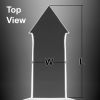
 A trapezoidal cross section of the AFM cantilever and therefore 30% wider (e.g. NCH) AFM cantilever detector side result in easier and faster laser adjustment. Additionally, because there is simply more space to place and reflect the laser beam, a higher SUM signal is reached.


 POINTPROBE®
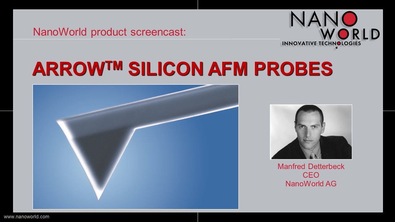
 ARROW™
 ULTRA-SHORT CANTILEVERS
 PYREX-NITRIDE
 COATINGS
