Feasibility of wear reduction for soft nanostructured thin film through enhanced elastic recoverability and contact stress relief

Over several decades many studies on the reduction of wear of mechanical systems have been conducted.
Methods to reduce wear are generally divided into the following categories: applying lubrication, coating with high-hardness materials, and surface texturing. *

Several studies have reported that coatings with higher hardness show more wear than those with lower hardness. From these reports, it is apparent that wear does not depend solely on the hardness of the surface.  Hence, there is a strong motivation for utilizing additional strategies for designing wear-resistive surfaces rather than only enhancing the hardness of the coating. *

In the article “Feasibility of wear reduction for soft nanostructured thin film through enhanced elastic recoverability and contact stress relief” Kuk-Jin Seo, Hyun-Joon Kim and Dae-Eun Kim show, that a soft, thin film comprising randomly aligned carbon nanotubes (CNTs) can reduce surface wear more effectively than a homogeneous thin film because of enhanced elastic recoverability and contact stress relief originating from its mesh structure. *

To investigate the wear characteristics of the mesh structure compared to those of the homogeneous thin film, multi-walled CNTs (MWCNTs) and diamond-like carbon (DLC) thin films were prepared to conduct nanoscale tribological experiments using atomic force microscopy (AFM). The MWCNT thin film showed unmeasurably low wear compared with the DLC thin film under a certain range of normal load. *

To demonstrate the wear reduction mechanism of the MWCNT thin film, its indentation and frictional behaviors were assessed. The indentation behavior of the MWCNT thin film revealed repetitive elastic deformation with a wide strain range and a significantly lower elastic modulus than that of the DLC thin film. The permanent deformation of the MWCNT thin film was observed through frictional experiments under relatively high normal load conditions. *

The presented results are expected to provide insights into the design of highly wear-resistant surfaces using nanostructures. *

The thickness and surface roughness of the MWCNT and DL thin films were measured using Atomic Force Microscopy. *

The force-displacement (F-D) curves were measured on the MWCNT thin film using the AFM to verify the mechanical behavior when indented by the zirconia microspheres that were used for wear and friction experiments. *

The adhesion forces between the thin films and zirconia microspheres were measured by observing the pull-off force of the F-D curve with the AFM. *

The adhesion force was measured using a colloidal AFM probe to aid the analysis of the tribological characteristics of the thin film. *

The pull-off forces for the DL specimens were obtained at 35 different locations with displacements of 50-200 nm. *

Diamond-coated AFM probes (NanoWorld Pointprobe® DT-NCHR ) were used for scanning, while non-coated silicon AFM probes with relatively high and low spring constants (NanoWorld Pointprobe® NCHR and CONTR) were used for the tribological experiments and specimen characterizations. *

Diamond-coated AFM probes (NanoWorld Pointprobe® DT-NCHR ) were used for scanning, while non-coated silicon AFM probes with relatively high and low spring constants (NanoWorld Pointprobe® NCHR and CONTR) were used for the tribological experiments and specimen characterizations.
Figure 6 from “Feasibility of wear reduction for soft nanostructured thin film through enhanced elastic recoverability and contact stress relief” by Kuk-Jin Seo et al.:
AFM images of wear tracks on the MWCNT thin film under test conditions of (a) 2,000 nN and 20,000 cycles, (b) 6,000 nN and 30,000 cycles, (c) 7,000 nN and 30,000 cycles, (d) 9,200 nN and 30,000 cycles, (e) 13,500 nN and 30,000 cycles, and (f) 28,000 nN and 30,000 cycles. Post-processed AFM images that subtracted the original image before each wear test under conditions of (g) 6,000 nN and 30,000 cycles, (h) 7,000 nN and 30,000 cycles, and (i) 28,000 nN and 30,000 cycles

*Kuk-Jin Seo, Hyun-Joon Kim and Dae-Eun Kim
Feasibility of wear reduction for soft nanostructured thin film through enhanced elastic recoverability and contact stress relief
Friction 11(7): 1292-1306 (2023)
DOI: https://doi.org/10.1007/s40544-022-0669-7

Please follow this external link to read the full article: https://rdcu.be/dejTa

The article “Feasibility of wear reduction for soft nanostructured thin film through enhanced elastic recoverability and contact stress relief” by Kuk-Jin Seo, Hyun-Joon Kim and Dae-Eun Kim is licensed under a Creative Commons Attribution 4.0 International License, which permits use, sharing, adaptation, distribution and reproduction in any medium or format, as long as you give appropriate credit to the original author(s) and the source, provide a link to the Creative Commons license, and indicate if changes were made. The images or other third-party material in this article are included in the article’s Creative Commons license, unless indicated otherwise in a credit line to the material. If material is not included in the article’s Creative Commons license and your intended use is not permitted by statutory regulation or exceeds the permitted use, you will need to obtain permission directly from the copyright holder. To view a copy of this license, visit https://creativecommons.org/licenses/by/4.0/.

Spherulite-like microstructure observed for spin-cast P(VDF-TrFE) thin films and their ferroelectric characteristics

Ferroelectric polymer thin films crystallize in different phases and microstructures depending on fabrication conditions such as annealing temperature or layer deposition technique.*

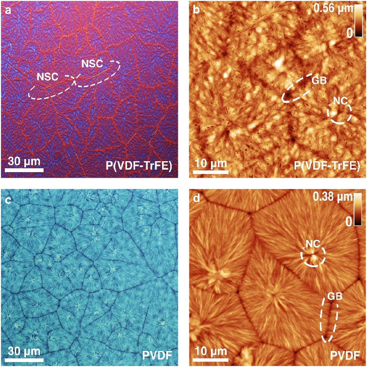
In the article “Spherulite-like microstructure observed for spin-cast P(VDF-TrFE) thin films and their ferroelectric characteristics” Davide Disnan, Jonas Hafner, Michael Schneider and Ulrich Schmid demonstrate how the morphology of spin-cast poly(vinylidene fluoride-trifluoroethylene) (P(VDF-TrFE)) thin films changes as a function of annealing temperature from rice-like to spherulite-like microstructure, whereas the latter morphology is closer to the crystallization characteristic of poly(vinylidene-fluoride) (PVDF).*

Thin films of PVDF and P(VDF-TrFE) were analyzed at the nanometre-scale using atomic force microscopy. *

NanoWorld Pyrex-Nitride PNP-TR AFM probes were used for the ferroelectric characterization of the polymer thin films by atomic force microscopy. *

The displacement of the metal-ferroelectric-metal structure in response to the electric field applied was measured at one single point in the centre of the capacitor. For that purpose, the AFM cantilever (NanoWorld PNP-TR with a spring constant of k = 0.32 N/m made of silicon nitride (non-conductive cantilever for avoiding electrical interference caused by ground loops) was used.*

The deflection during the electrical stimulation was calibrated through the measurement of the inverse optical lever sensitivity of the probe. In order to avoid significant indentation effects, the silicon wafer surface surrounding the capacitor structure was used to land the cantilever for the calibration. *

Fig. 1 from «Spherulite-like microstructure observed for spin-cast P(VDF-TrFE) thin films and their ferroelectric characteristics» by D. Disnan et al: Spherulite-like microstructure of P(VDF-TrFE) and spherulite microstructure of PVDF. a, b Optical micrograph and AFM height image of the spherulite-like microstructure of P(VDF-TrFE). Features like needle-shaped crystals (NSC), nucleation centres (NC) and grain boundaries (GB) are highlighted on the spherulite-like microstructure surface. C ,d Analog for the spherulite microstructure of PVDF. NanoWorld Pyrex-Nitride AFM probes of the PNP-TR type were used for the Ferroelectric characterization of the polymer thin films.
Fig. 1 from «Spherulite-like microstructure observed for spin-cast P(VDF-TrFE) thin films and their ferroelectric characteristics» by D. Disnan et al:
Spherulite-like microstructure of P(VDF-TrFE) and spherulite microstructure of PVDF. a, b Optical micrograph and AFM height image of the spherulite-like microstructure of P(VDF-TrFE). Features like needle-shaped crystals (NSC), nucleation centres (NC) and grain boundaries (GB) are highlighted on the spherulite-like microstructure surface. C ,d Analog for the spherulite microstructure of PVDF.

Please follow the external link to read the full article:

*Davide Disnan, Jonas Hafner, Michael Schneider and Ulrich Schmid
Spherulite-like microstructure observed for spin-cast P(VDF-TrFE) thin films and their ferroelectric characteristics
Polymer, Volume 272, 17 April 2023, 125840
DOI: https://doi.org/10.1016/j.polymer.2023.125840

The article “Spherulite-like microstructure observed for spin-cast P(VDF-TrFE) thin films and their ferroelectric characteristics” by Davide Disnan, Jonas Hafner, Michael Schneider and Ulrich Schmid is licensed under a Creative Commons Attribution 4.0 International License, which permits use, sharing, adaptation, distribution and reproduction in any medium or format, as long as you give appropriate credit to the original author(s) and the source, provide a link to the Creative Commons license, and indicate if changes were made. The images or other third party material in this article are included in the article’s Creative Commons license, unless indicated otherwise in a credit line to the material. If material is not included in the article’s Creative Commons license and your intended use is not permitted by statutory regulation or exceeds the permitted use, you will need to obtain permission directly from the copyright holder. To view a copy of this license, visit https://creativecommons.org/licenses/by/4.0/.


Impact of annealing on electric and elastic properties of 10-nm Hf0.5Zr0.5O2 films prepared on Si by sputtering

HfO2-based films are important materials used in broad range of electronic applications from high-performance transistors and memory cells, to thermoelectric and energy harvesting elements. *

In the article “Impact of annealing on electric and elastic properties of 10-nm Hf0.5Zr0.5O2 films prepared on Si by sputtering” Leonid Bolotov, Shinji Migita, Ryouta Fujio, Manabu Ishimaru, Shogo Hatayama and Noriyuki Uchida described how they used scanning probe methods to make nanoscale comparison of chemical composition, surface morphology, the elastic modulus and the surface potential of bare 10-nm thick Hf0.5Zr0.5O2 films prepared on Si by a carbon-free sputtering process. *

NanoWorld conductive platinum iridium5 coated Pointprobe® EFM AFM probes were used for the electrostatic force microscopy (EFM). *

The composition mapping confirmed uniform distribution of Hf and Zr in the film along wafer size. Suppression of the monoclinic phase in films annealed at 600 – 800 °C had strong impact on spatial variations of film properties. Small surface roughness, large electric domain sizes (50–200 nm at 700 °C) and small fluctuations of the surface potential (40–50 meV) in Si coated with the films are appealing for gate-stack applications. Films annealed at 600-700 °C showed the elastic modulus of about 169 GPa and the ferroelectric polarization reversal at a field of ~1 MV/cm as observed by nanoscale poling with a Pt-coated scanning probe. In contrast, properties of films annealing at 800 °C were affected by growth of thick interfacial oxide layer. *

The nanoscale approach presented in the article is beneficial in optimizing of physical and mechanical properties of thin dielectric films. *

Fig. 3 from Leonid Bolotov et al. “Impact of annealing on electric and elastic properties of 10-nm Hf0.5Zr0.5O2 films prepared on Si by sputtering”: AFM topographs (a, c) and CPD maps (b, d) of 10 nm Hf0.5Zr0.5O2 films on Si: as-grown film (a, b), and annealed at 700 °C (c, d). Rectangular shapes in (c, d) outline one domain. Scale bars are 200 nm. NanoWorld conductive platinum iridium5 coated Pointprobe® EFM AFM probes were used for the electrostatic force microscopy (EFM).
Fig. 3 from Leonid Bolotov et al. “Impact of annealing on electric and elastic properties of 10-nm Hf0.5Zr0.5O2 films prepared on Si by sputtering”:
AFM topographs (a, c) and CPD maps (b, d) of 10 nm Hf0.5Zr0.5O2 films on Si: as-grown film (a, b), and annealed at 700 °C (c, d). Rectangular shapes in (c, d) outline one domain. Scale bars are 200 nm.

*Leonid Bolotov, Shinji Migita, Ryouta Fujio, Manabu Ishimaru, Shogo Hatayama and Noriyuki Uchida
Impact of annealing on electric and elastic properties of 10-nm Hf0.5Zr0.5O2 films prepared on Si by sputtering
Microelectronic Engineering, Volume 258, 1 April 2022, 111770
DOI: https://doi.org/10.1016/j.mee.2022.111770

Open Access The article “Impact of annealing on electric and elastic properties of 10-nm Hf0.5Zr0.5O2 films prepared on Si by sputtering” by Leonid Bolotov, Shinji Migita, Ryouta Fujio, Manabu Ishimaru, Shogo Hatayama and Noriyuki Uchida is licensed under a Creative Commons Attribution 4.0 International License, which permits use, sharing, adaptation, distribution and reproduction in any medium or format, as long as you give appropriate credit to the original author(s) and the source, provide a link to the Creative Commons license, and indicate if changes were made. The images or other third party material in this article are included in the article’s Creative Commons license, unless indicated otherwise in a credit line to the material. If material is not included in the article’s Creative Commons license and your intended use is not permitted by statutory regulation or exceeds the permitted use, you will need to obtain permission directly from the copyright holder. To view a copy of this license, visit http://creativecommons.org/licenses/by/4.0/.