Real-time tracking of ionic nano-domains under shear flow

The behaviour of ions at solid–liquid interfaces underpins countless phenomena, from the conduction of nervous impulses to charge transfer in solar cells. In most cases, ions do not operate as isolated entities, but in conjunction with neighbouring ions and the surrounding solution. In aqueous solutions, recent studies suggest the existence of group dynamics through water-mediated clusters but results allowing direct tracking of ionic domains with atomic precision are scarce. *

Atomic force microscopy (AFM) can image single ions adsorbed at various solid–liquid interfaces. One of the main advantages of the technique is its ability to probe individual ions in-situ but with local contextual information about the interface over tens of nanometres at the point of measurement.*

High-speed atomic force microscopy (HS-AFM) operates similarly to standard AFM but with enhanced temporal resolution and can capture images at video rate, making it possible to track many molecular processes in real-time.*

In the article “Real-time tracking of ionic nano-domains under shear flow” Clodomiro Cafolla and Kislon Voïtchovsky use high-speed atomic force microscopy to track the evolution of Rb+, K+, Na+ and Ca2+ nano-domains containing 20 to 120 ions adsorbed at the surface of mica in aqueous solution. The interface is exposed to a shear flow able to influence the lateral motion of single ions and clusters. *

They report the achievement of single-ion spatial resolution with ~ 2 s temporal resolution.*

During the measurements, the AFM cantilever and the sample were fully immersed in the aqueous ionic solution of interest. The AFM probes used were NanoWorld Arrow-UHF ultra-high frequency AFM cantilevers. *

The results presented in the article provide some quantitative insights into the relationship between single ion properties and group dynamics at the solid–liquid interface in the presence of a microscale shear flow, with potential technological applications from manufacturing biomedical devices to enhancing the performance of aqueous ion-batteries.*
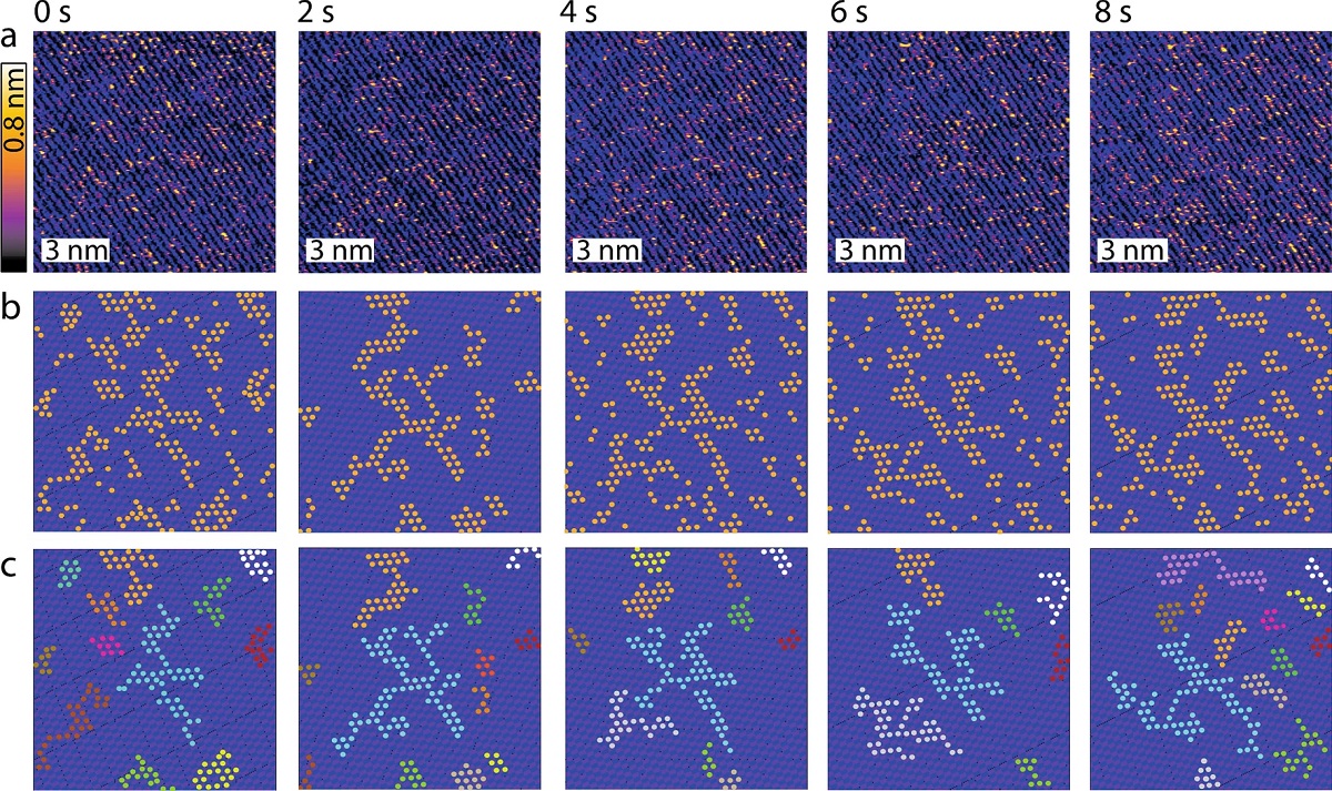
Figure 1 from “Real-time tracking of ionic nano-domains under shear flow” by Clodomiro Cafolla and Kislon Voïtchovsky: Example of time evolution for adsorbed Rb+ ions at the mica-water interface in the presence of a shear flow. (a) A time-lapse sequence shows consecutive high-resolution HS-AFM topographical images of Rb+ ions at the interface between mica and a 5 mM RbCl aqueous solution. Rb+ ions appear as bright orange-yellow protrusions standing taller than the mica surface (purple-black). Periodic rows and larger domains are clearly visible as well as singly adsorbed rubidium ions. (b) Representative image analysis highlighting Rb+ ions as orange markers (obtained by thresholding) and the idealised underlying lattice derived by inverse Fourier transform of the filtered power spectrum in each image of (a) (see ESI Section 3 for details on the procedure). (c) The algorithm automatically associates neighbouring ions (within distances < 0.52 nm) to the same cluster. Domains smaller than 5 ions are discarded here. The different clusters derived in each image are highlighted using different colours, keeping for each cluster the same colour over time. The cyan-coloured cluster offers a good example of temporal evolution. The scale bars in (a–c) represent 3 nm and the z-scale in (a) corresponds to 0.8 nm. NanoWorld Arrow-UHF ultra-high speed AFM probes were used for the high-speed atomic force microscopy (HS-AFM).
Figure 1 from “Real-time tracking of ionic nano-domains under shear flow” by Clodomiro Cafolla and Kislon Voïtchovsky:
Example of time evolution for adsorbed Rb+ ions at the mica-water interface in the presence of a shear flow. (a) A time-lapse sequence shows consecutive high-resolution HS-AFM topographical images of Rb+ ions at the interface between mica and a 5 mM RbCl aqueous solution. Rb+ ions appear as bright orange-yellow protrusions standing taller than the mica surface (purple-black). Periodic rows and larger domains are clearly visible as well as singly adsorbed rubidium ions. (b) Representative image analysis highlighting Rb+ ions as orange markers (obtained by thresholding) and the idealised underlying lattice derived by inverse Fourier transform of the filtered power spectrum in each image of (a) (see ESI Section 3 for details on the procedure). (c) The algorithm automatically associates neighbouring ions (within distances < 0.52 nm) to the same cluster. Domains smaller than 5 ions are discarded here. The different clusters derived in each image are highlighted using different colours, keeping for each cluster the same colour over time. The cyan-coloured cluster offers a good example of temporal evolution. The scale bars in (a–c) represent 3 nm and the z-scale in (a) corresponds to 0.8 nm.

*Clodomiro Cafolla and Kislon Voïtchovsky
Real-time tracking of ionic nano-domains under shear flow
Nature Scientific Reports volume 11, Article number: 19540 (2021)
DOI: https://doi.org/10.1038/s41598-021-98137-y

Please follow this external link to read the full article: https://rdcu.be/cPRBu

Open Access The article “Real-time tracking of ionic nano-domains under shear flow” by Clodomiro Cafolla and Kislon Voïtchovsky is licensed under a Creative Commons Attribution 4.0 International License, which permits use, sharing, adaptation, distribution and reproduction in any medium or format, as long as you give appropriate credit to the original author(s) and the source, provide a link to the Creative Commons license, and indicate if changes were made. The images or other third party material in this article are included in the article’s Creative Commons license, unless indicated otherwise in a credit line to the material. If material is not included in the article’s Creative Commons license and your intended use is not permitted by statutory regulation or exceeds the permitted use, you will need to obtain permission directly from the copyright holder. To view a copy of this license, visit http://creativecommons.org/licenses/by/4.0/.

Magnetic reversal in perpendicularly magnetized antidot arrays with intrinsic and extrinsic defects

Defects can significantly affect performance of nanopatterned magnetic devices, therefore their influence on the material properties has to be understood well before the material is used in technological applications. However, this is experimentally challenging due to the inability of the control of defect characteristics in a reproducible manner.*

In “Magnetic reversal in perpendicularly magnetized antidot arrays with intrinsic and extrinsic defects» Michal Krupinski, Pawel Sobieszczyk, Piotr Zieliński and Marta Marszałek construct a micromagnetic model, which accounts for intrinsic and extrinsic defects associated with the polycrystalline nature of the material and with corrugated edges of nanostructures.*

The findings described in their article show that magnetic properties and domain configuration in nanopatterned systems are strongly determined by the defects, the heterogeneity of the nanostructure sizes and edge corrugations, and that such imperfections play a key role in the processes of magnetic reversal.*

The magnetic imaging described in the article cited above was performed using NanoWorld MFMR AFM probes for magnetic force microscopy (MFMR).

Figure 8 from “Magnetic reversal in perpendicularly magnetized antidot arrays with intrinsic and extrinsic defects” by Michal Krupinski et al.:
(a) MFM image for an array with an antidot diameter 182 nm taken in zero field after ac demagnetization. Selected domain walls were marked with a blue line. (b) Simulated MFM image for an antidot diameter of 185 nm corresponding to the magnetic moment configuration depicted in Fig. 6b. The MFM tip distance from the sample surface was 180 nm.

*Michal Krupinski, Pawel Sobieszczyk, Piotr Zieliński and Marta Marszałek
Magnetic reversal in perpendicularly magnetized antidot arrays with intrinsic and extrinsic defects
Nature Scientific Reports volume 9, Article number: 13276 (2019)
DOI: https://doi.org/10.1038/s41598-019-49869-5

Please follow this external link to read the full article https://rdcu.be/bYXYP

Open Access: The article “Magnetic reversal in perpendicularly magnetized antidot arrays with intrinsic and extrinsic defects” by Michal Krupinski, Pawel Sobieszczyk, Piotr Zieliński and Marta Marszałek is licensed under a Creative Commons Attribution 4.0 International License, which permits use, sharing, adaptation, distribution and reproduction in any medium or format, as long as you give appropriate credit to the original author(s) and the source, provide a link to the Creative Commons license, and indicate if changes were made. The images or other third party material in this article are included in the article’s Creative Commons license, unless indicated otherwise in a credit line to the material. If material is not included in the article’s Creative Commons license and your intended use is not permitted by statutory regulation or exceeds the permitted use, you will need to obtain permission directly from the copyright holder. To view a copy of this license, visit http://creativecommons.org/licenses/by/4.0/.

Magnetization-polarization cross-control near room temperature in hexaferrite single crystals

In their publication “Magnetization-polarization cross-control near room temperature in hexaferrite single crystals” V. Kocsis, T. Nakajima, M. Matsuda, A. Kikkawa, Y. Kaneko, J. Takashima, K. Kakurai, T. Arima, F. Kagawa, Y. Tokunaga, Y. Tokura and Y. Taguchi report that they have successfully stabilized a simultaneously ferrimagnetic and ferroelectric phase in a Y-type hexaferrite single crystal up to 450 K, and demonstrated the reversal of large non-volatile M by E field close to room temperature. Manipulation of the magnetic domains by E field was directly visualized at room temperature by using magnetic force microscopy.*

NanoWorld MFMR AFM probes with a hard magnetic coating were used for the magnetic force microscopy measurements described in this article.

Figure 5 from “Magnetization-polarization cross-control near room temperature in hexaferrite single crystals” by V. Kocsis et al.: Real-space magnetic force microscopy (MFM) images. The MFM images were taken on the same 10 × 10 μm2 region of a BSCFAO crystal with an ac face (see Supplementary Figs. 3, 9 and 10) at room temperature. Prior to the MFM measurements, the sample was poled to a single-domain ME state using (+E0, +H0) poling fields in a E ⊥ H; E, H ⊥ c configuration. Panel a shows the changes in the magnetic domain pattern caused by two successive applications of the E field with different signs (the initial state is labeled as the 0th). The images include small regions, R1 and R2, where two representative cases of DW motion are observed. Around R1, the negatively magnetized domain (denoted with blue color, MFM phase shift Δφ < 0) expands and shrinks along the c-axis upon the first and second applications of E-field, respectively. On the other hand, around R2, a positively magnetized domain (denoted with red color, Δφ > 0) is pushed into the view area from the upper side along the ab plane. These two cases are further displayed as line profiles of the MFM phase shift (Δφ) data along the b A−A′ and c B−B′ lines. Panels d, e show the schematic illustration of these two cases of domain wall motions for the second E-field switch, respectively. NanoWorld MFMR AFM probes were used for the magnetic force microscopy.
Figure 5 from “Magnetization-polarization cross-control near room temperature in hexaferrite single crystals” by V. Kocsis et al.: Real-space magnetic force microscopy (MFM) images. The MFM images were taken on the same 10 × 10 μm2 region of a BSCFAO crystal with an ac face (see Supplementary Figs. 3, 9 and 10) at room temperature. Prior to the MFM measurements, the sample was poled to a single-domain ME state using (+E0, +H0) poling fields in a E ⊥ H; E, H ⊥ c configuration. Panel a shows the changes in the magnetic domain pattern caused by two successive applications of the E field with different signs (the initial state is labeled as the 0th). The images include small regions, R1 and R2, where two representative cases of DW motion are observed. Around R1, the negatively magnetized domain (denoted with blue color, MFM phase shift Δφ < 0) expands and shrinks along the c-axis upon the first and second applications of E-field, respectively. On the other hand, around R2, a positively magnetized domain (denoted with red color, Δφ > 0) is pushed into the view area from the upper side along the ab plane. These two cases are further displayed as line profiles of the MFM phase shift (Δφ) data along the b A−A′ and c B−B′ lines. Panels d, e show the schematic illustration of these two cases of domain wall motions for the second E-field switch, respectively.

*V. Kocsis, T. Nakajima, M. Matsuda, A. Kikkawa, Y. Kaneko, J. Takashima, K. Kakurai, T. Arima, F. Kagawa, Y. Tokunaga, Y. Tokura, Y. Taguchi
Magnetization-polarization cross-control near room temperature in hexaferrite single crystals
Nature Communications, volume 10, Article number: 1247 (2019)
DOI: https://doi.org/10.1038/s41467-019-09205-x

Please follow this external link to the full article: https://www.nature.com/articles/s41467-019-09205-x

Open Access The article ” Magnetization-polarization cross-control near room temperature in hexaferrite single crystals” by V. Kocsis et al. is licensed under a Creative Commons Attribution 4.0 International License, which permits use, sharing, adaptation, distribution and reproduction in any medium or format, as long as you give appropriate credit to the original author(s) and the source, provide a link to the Creative Commons license, and indicate if changes were made. The images or other third party material in this article are included in the article’s Creative Commons license, unless indicated otherwise in a credit line to the material. If material is not included in the article’s Creative Commons license and your intended use is not permitted by statutory regulation or exceeds the permitted use, you will need to obtain permission directly from the copyright holder. To view a copy of this license, visit http://creativecommons.org/licenses/by/4.0/.