C-Axis Textured, 2–3 μm Thick Al0.75Sc0.25N Films Grown on Chemically Formed TiN/Ti Seeding Layers for MEMS Applications

In the search for lead-free, Si-microfabrication-compatible piezoelectric materials, thin films of scandium-doped aluminum nitride (Al,Sc)N are of great interest for use in actuators, energy harvesting, and micro-electromechanical-systems (MEMS).*

While the piezoelectric response of AlN increases upon doping with Sc, difficulties are encountered during film preparation because, as bulk solids with completely different structures and large differences in cation radii, ScN (rock salt, cubic) and AlN (wurtzite, hexagonal) are immiscible. *

Consequently, (Al,Sc)N is inherently thermodynamically unstable and prone to phase segregation. Film preparation is further complicated by the technological requirement for polar [001] or [00 1̲] out-of-plane texture, which is achieved using a seeding layer.*

In the article “C-Axis Textured, 2–3 μm Thick Al0.75Sc0.25N Films Grown on Chemically Formed TiN/Ti Seeding Layers for MEMS Applications” Asaf Cohen, Hagai Cohen, Sidney R. Cohen, Sergey Khodorov, Yishay Feldman, Anna Kossoy, Ifat Kaplan-Ashiri, Anatoly Frenkel, Ellen Wachtel, Igor Lubomirsky and David Ehre propose a protocol for successfully depositing [001] textured, 2–3 µm thick films of Al0.75Sc0.25N.*

The procedure relies on the fact that sputtered Ti is [001]-textured α-phase (hcp). Diffusion of nitrogen ions into the α-Ti film during reactive sputtering of Al0.75,Sc0.25N likely forms a [111]-oriented TiN intermediate layer. The lattice mismatch of this very thin film with Al0.75Sc0.25N is ~3.7%, providing excellent conditions for epitaxial growth. In contrast to earlier reports, the Al0.75Sc0.25N films prepared in the current study are Al-terminated. Low growth stress (<100 MPa) allows films up to 3 µm thick to be deposited without loss of orientation or decrease in piezoelectric coefficient. *

An advantage of the proposed technique is that it is compatible with a variety of substrates commonly used for actuators or MEMS, as demonstrated here for both Si wafers and D263 borosilicate glass. Additionally, thicker films can potentially lead to increased piezoelectric stress/strain by supporting application of higher voltage, but without increase in the magnitude of the electric field. *

SEM, AFM, EDS, XRD and XPS techniques were used for the film characterization. For the nanoscale topography maps with atomic force microscopy (AFM) NanoWorld Pyrex-Nitride series PNP-TRS silicon nitride AFM probes were used in peak-force tapping mode. *

Figure 3 from Asaf Cohen et al. “C-Axis Textured, 2–3 μm Thick Al0.75Sc0.25N Films Grown on Chemically Formed TiN/Ti Seeding Layers for MEMS Applications”: AFM images of (a) a (100) silicon wafer following cleaning procedures as described in the Materials and Methods section; (b) 50 nm-thick Ti film deposited on the wafer at 300 K; (c) the same film following exposure to N2 plasma at 673 K for 30 min. For the nanoscale topography maps with atomic force microscopy (AFM) NanoWorld Pyrex-Nitride PNP-TRS AFM probes were used in peak-force tapping mode1. *
Figure 3 from Asaf Cohen et al. “C-Axis Textured, 2–3 μm Thick Al0.75Sc0.25N Films Grown on Chemically Formed TiN/Ti Seeding Layers for MEMS Applications”: AFM images of (a) a (100) silicon wafer following cleaning procedures as described in the Materials and Methods section; (b) 50 nm-thick Ti film deposited on the wafer at 300 K; (c) the same film following exposure to N2 plasma at 673 K for 30 min.

*Asaf Cohen, Hagai Cohen, Sidney R. Cohen, Sergey Khodorov, Yishay Feldman, Anna Kossoy, Ifat Kaplan-Ashiri, Anatoly Frenkel, Ellen Wachtel, Igor Lubomirsky and David Ehre
C-Axis Textured, 2–3 μm Thick Al0.75Sc0.25N Films Grown on Chemically Formed TiN/Ti Seeding Layers for MEMS Applications
Sensors 2022, 22, 7041
DOI: https://doi.org/10.3390/s22187041

The article “C-Axis Textured, 2–3 μm Thick Al0.75Sc0.25N Films Grown on Chemically Formed TiN/Ti Seeding Layers for MEMS Applications” by Asaf Cohen, Hagai Cohen, Sidney R. Cohen, Sergey Khodorov, Yishay Feldman, Anna Kossoy, Ifat Kaplan-Ashiri, Anatoly Frenkel, Ellen Wachtel, Igor Lubomirsky and David Ehre is licensed under a Creative Commons Attribution 4.0 International License, which permits use, sharing, adaptation, distribution and reproduction in any medium or format, as long as you give appropriate credit to the original author(s) and the source, provide a link to the Creative Commons license, and indicate if changes were made. The images or other third-party material in this article are included in the article’s Creative Commons license, unless indicated otherwise in a credit line to the material. If material is not included in the article’s Creative Commons license and your intended use is not permitted by statutory regulation or exceeds the permitted use, you will need to obtain permission directly from the copyright holder. To view a copy of this license, visit https://creativecommons.org/licenses/by/4.0/.

1Peak Force Tapping® is a registered trademark of Bruker Corporation.

Spherulite-like microstructure observed for spin-cast P(VDF-TrFE) thin films and their ferroelectric characteristics

Ferroelectric polymer thin films crystallize in different phases and microstructures depending on fabrication conditions such as annealing temperature or layer deposition technique.*

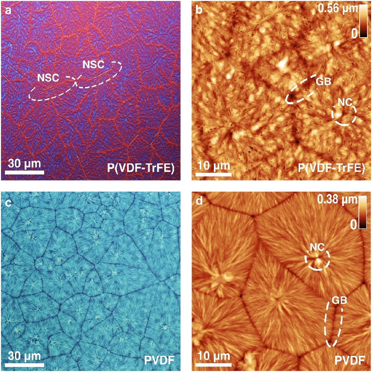
In the article “Spherulite-like microstructure observed for spin-cast P(VDF-TrFE) thin films and their ferroelectric characteristics” Davide Disnan, Jonas Hafner, Michael Schneider and Ulrich Schmid demonstrate how the morphology of spin-cast poly(vinylidene fluoride-trifluoroethylene) (P(VDF-TrFE)) thin films changes as a function of annealing temperature from rice-like to spherulite-like microstructure, whereas the latter morphology is closer to the crystallization characteristic of poly(vinylidene-fluoride) (PVDF).*

Thin films of PVDF and P(VDF-TrFE) were analyzed at the nanometre-scale using atomic force microscopy. *

NanoWorld Pyrex-Nitride PNP-TR AFM probes were used for the ferroelectric characterization of the polymer thin films by atomic force microscopy. *

The displacement of the metal-ferroelectric-metal structure in response to the electric field applied was measured at one single point in the centre of the capacitor. For that purpose, the AFM cantilever (NanoWorld PNP-TR with a spring constant of k = 0.32 N/m made of silicon nitride (non-conductive cantilever for avoiding electrical interference caused by ground loops) was used.*

The deflection during the electrical stimulation was calibrated through the measurement of the inverse optical lever sensitivity of the probe. In order to avoid significant indentation effects, the silicon wafer surface surrounding the capacitor structure was used to land the cantilever for the calibration. *

Fig. 1 from «Spherulite-like microstructure observed for spin-cast P(VDF-TrFE) thin films and their ferroelectric characteristics» by D. Disnan et al: Spherulite-like microstructure of P(VDF-TrFE) and spherulite microstructure of PVDF. a, b Optical micrograph and AFM height image of the spherulite-like microstructure of P(VDF-TrFE). Features like needle-shaped crystals (NSC), nucleation centres (NC) and grain boundaries (GB) are highlighted on the spherulite-like microstructure surface. C ,d Analog for the spherulite microstructure of PVDF. NanoWorld Pyrex-Nitride AFM probes of the PNP-TR type were used for the Ferroelectric characterization of the polymer thin films.
Fig. 1 from «Spherulite-like microstructure observed for spin-cast P(VDF-TrFE) thin films and their ferroelectric characteristics» by D. Disnan et al:
Spherulite-like microstructure of P(VDF-TrFE) and spherulite microstructure of PVDF. a, b Optical micrograph and AFM height image of the spherulite-like microstructure of P(VDF-TrFE). Features like needle-shaped crystals (NSC), nucleation centres (NC) and grain boundaries (GB) are highlighted on the spherulite-like microstructure surface. C ,d Analog for the spherulite microstructure of PVDF.

Please follow the external link to read the full article:

*Davide Disnan, Jonas Hafner, Michael Schneider and Ulrich Schmid
Spherulite-like microstructure observed for spin-cast P(VDF-TrFE) thin films and their ferroelectric characteristics
Polymer, Volume 272, 17 April 2023, 125840
DOI: https://doi.org/10.1016/j.polymer.2023.125840

The article “Spherulite-like microstructure observed for spin-cast P(VDF-TrFE) thin films and their ferroelectric characteristics” by Davide Disnan, Jonas Hafner, Michael Schneider and Ulrich Schmid is licensed under a Creative Commons Attribution 4.0 International License, which permits use, sharing, adaptation, distribution and reproduction in any medium or format, as long as you give appropriate credit to the original author(s) and the source, provide a link to the Creative Commons license, and indicate if changes were made. The images or other third party material in this article are included in the article’s Creative Commons license, unless indicated otherwise in a credit line to the material. If material is not included in the article’s Creative Commons license and your intended use is not permitted by statutory regulation or exceeds the permitted use, you will need to obtain permission directly from the copyright holder. To view a copy of this license, visit https://creativecommons.org/licenses/by/4.0/.


Molecular and nanoscale evaluation of N-cadherin expression in invasive bladder cancer cells under control conditions or GW501516 exposure

N-cadherin is a transmembrane glycoprotein expressed by mesenchymal origin cells and is located at the adherens junctions. It regulates also cell motility and contributes to cell signaling.*

A pharmacological approach to inhibit N-cadherin expression or to block its function could be relevant to prevent disease progression and metastasis development.*

In the article “Molecular and nanoscale evaluation of N-cadherin expression in invasive bladder cancer cells under control conditions or GW501516 exposure” Céline Elie-Caille, Isabelle Lascombe, Adeline Péchery, Hugues Bittard and Sylvie Fauconnet, describe how they aimed at exploring the expression level of N-cadherin in invasive bladder cancer cells upon GW501516 exposure by both molecular biology techniques such as RTqPCR and Western blotting and atomic force microscopy (AFM) using an AFM tip functionalized with a monoclonal antibody directed against this adhesion molecule. *

The Atomic Force Microscope is a mighty nanoanalytical tool for studying biological samples under liquid, in pathological or physiological conditions, and at the scale of a single cell. It allows to characterize cells and their modification upon drug exposure or function alteration, in terms of cell surface topography or cell adhesion. *

The authors demonstrated for the first time, that the PPARβ/δ activator from a concentration of 15 µM decreased the full length N-cadherin at the mRNA and protein level and significantly reduced its cell surface coverage through the measurements of the interaction forces involving this adhesion molecule. *

Using atomic force microscopy the authors carried out a morphological and topographical analysis on bladder cancer cells of different histologic grade. *

AFM imaging was carried out in contact mode on fixed cells (with an applied force of 0.1 V), the QI mode was used for alive cell imaging, all in liquid. *

Force spectroscopy in force mapping was used for cadherin/anti-cadherin antibody measurement interactions and cadherin mapping on cells. *

NanoWorld Pyrex-Nitride PNP-TR triangular shaped silicon nitride cantilevers ( CB2 with a typical spring constant of 0.08 N/m ) were used.

For force mapping the AFM cantilevers were calibrated. The AFM probes, made of silicon nitride, were functionalized by 1% APTES (3-(Aminopropyl)triethoxysilane) in toluene during 2 h, washed extensively with toluene, and then with ethanol.
The second step consisted in an incubation in 0.2% glutaraldehyde solution during 10 min, followed by extensive washing with water. A naked AFM tip was used as a negative control.
The modified AFM tips were then incubated in 50 µg/mL primary antibody solution (N-cadherin GC-4 clone directed against the extracellular domain, N-cadherin 3B9 clone directed against the intracellular domain, E-cadherin HECD-1 clone directed against the extracellular domain) during 30 min, then washed with PBS 1X.
Finally, the functionalized AFM tip was saturated by incubation in 2 mg/mL RSA (rat serum albumin) solution during 30 min. *

Quantitative imaging AFM mode enabled to register more than hundred force spectroscopy curves per condition. The curves registered on cells were overlayed in order to highlight a specific pattern and the interaction peak areas were measured. *

Figure 1 from “Molecular and nanoscale evaluation of N-cadherin expression in invasive bladder cancer cells under control conditions or GW501516 exposure” by Céline Elie-Caille et al.:
T24 and RT4 bladder cancer cell morphology and topography. a Images from control confluent cells by phase contrast microscopy. Scale bars: 200 µm. b, c AFM images obtained on control confluent cells, after glutaraldehyde fixation, in contact mode in liquid. b AFM height images. c AFM deflection images. Scale bars: 10 µm
NanoWorld Pyrex-Nitride triangular PNP-TR silicon nitride AFM probes were used for the atomic force microscopy.
Figure 1 from “Molecular and nanoscale evaluation of N-cadherin expression in invasive bladder cancer cells under control conditions or GW501516 exposure” by Céline Elie-Caille et al.:
T24 and RT4 bladder cancer cell morphology and topography. a Images from control confluent cells by phase contrast microscopy. Scale bars: 200 µm. b, c AFM images obtained on control confluent cells, after glutaraldehyde fixation, in contact mode in liquid. b AFM height images. c AFM deflection images. Scale bars: 10 µm

* Céline Elie-Caille, Isabelle Lascombe, Adeline Péchery, Hugues Bittard amd Sylvie Fauconnet
Molecular and nanoscale evaluation of N-cadherin expression in invasive bladder cancer cells under control conditions or GW501516 exposure
Molecular and Cellular Biochemistry (2020) 471:113–127
DOI: https://doi.org/10.1007/s11010-020-03771-1

Please follow this external link to read the full article: https://link.springer.com/article/10.1007/s11010-020-03771-1

Open Access : The article “Molecular and nanoscale evaluation of N-cadherin expression in invasive bladder cancer cells under control conditions or GW501516 exposure” by Céline Elie-Caille, Isabelle Lascombe, Adeline Péchery, Hugues Bittard and Sylvie Fauconnet is licensed under a Creative Commons Attribution 4.0 International License, which permits use, sharing, adaptation, distribution and reproduction in any medium or format, as long as you give appropriate credit to the original author(s) and the source, provide a link to the Creative Commons license, and indicate if changes were made. The images or other third party material in this article are included in the article’s Creative Commons license, unless indicated otherwise in a credit line to the material. If material is not included in the article’s Creative Commons license and your intended use is not permitted by statutory regulation or exceeds the permitted use, you will need to obtain permission directly from the copyright holder. To view a copy of this license, visit https://creativecommons.org/licenses/by/4.0/.