Electrochemical detection of quinone reduced by Complex I Complex II and Complex III in full mitochondrial membranes

In the last decades enormous advances have been made in characterizing the atomic and molecular structure of respiratory chain supercomplexes. *

However, it still remains a challenge to stitch this refined spatial atomistic description with functional information provided by biochemical studies of isolated protein material. Development of functional assays that detect respiratory chain complexes in their native membrane environment contribute to address the open questions related to the role played by their association and interactions. *

In the article “Electrochemical detection of quinone reduced by Complex I Complex II and Complex III in full mitochondrial membranes” Daniel G. Cava, Julia Alvarez-Malmagro, Paolo Natale, Sandra López-Calcerrada, Iván López-Montero, Cristina Ugalde, Jose Maria Abad, Marcos Pita, Antonio L. De Lacey and Marisela Vélez present a characterization assay in which a functionalized gold electrode is modified with mitochondrial membrane fragments that allows monitoring electrochemically the activity of different respiratory chain complexes immersed in the mitochondrial membrane. *

Daniel G. Cava  et al. measure the intensity of the reducing current of the electron mediator CoQ1 at the electrode surface and its variation upon addition of the corresponding enzymatic substrates. The activities of Complex I, Complex II and Complex III were monitored by the way in which they reduce the current, reflecting the amount of quinone reduced by the complexes in the presence of their substrates. *

The authors detect that CoQ1H2 produced by Complex I remains partially trapped within the membrane and is more easily oxidized by Complex III or the electrode than the quinone reduced by Complex II. *

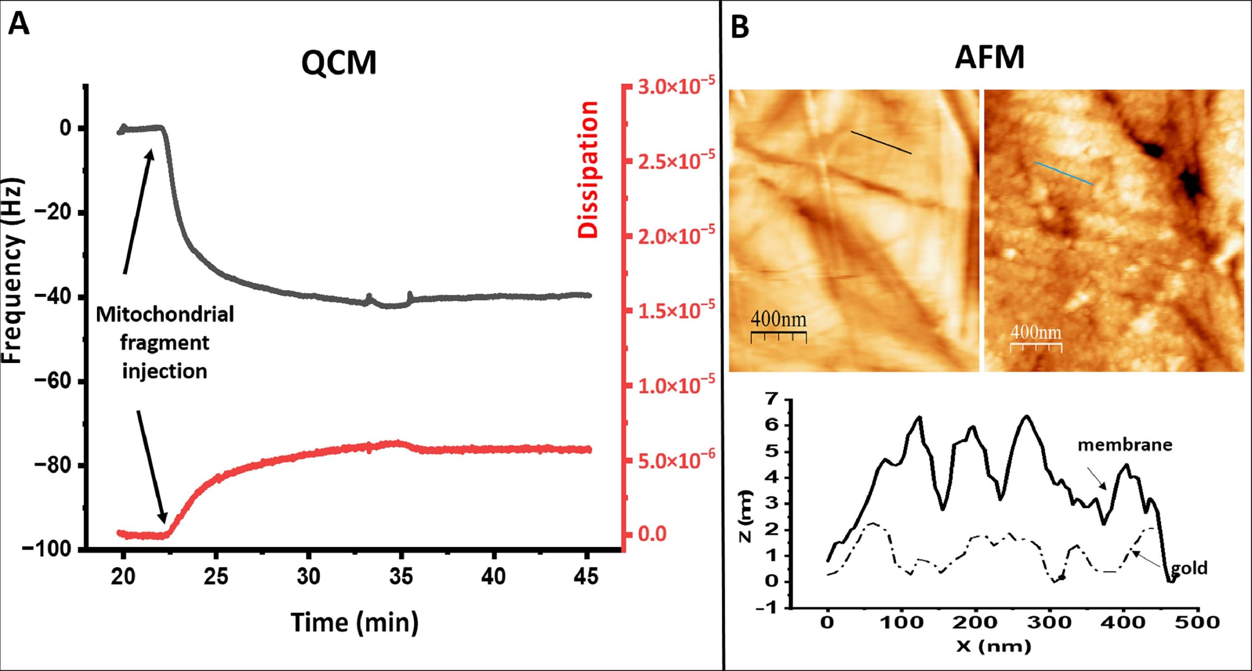
Atomic Force Microscopy (AFM) was used to image the topography of the membrane modified electrode. NanoWorld Pyrex-Nitride Silicon-Nitride AFM probes (PNP-DB, diving board shaped cantilevers, the short AFM cantilever with a typical force constant of 0.48 N/m and 67 kHz resonance frequency) were used. *

The surfaces analysed were the electrodes. The two surfaces imaged are the same previously polished electrodes used for electrochemical measurements. The microscope sample holder was adapted in-home to support the electrodes. Two surfaces were analysed: the polished gold functionalized with 4-aminothiophenol and the electrode after incubation with mitochondria subparticles prepared similarly to the electrodes used for the electrochemical measurements.*

Fig. 2 from Daniel G. Cava et al 2024 “Electrochemical detection of quinone reduced by Complex I Complex II and Complex III in full mitochondrial membranes” QCM and AFM characterization of modified gold. Panel A shows the frequency (left, black) and dissipation (right red) changes detected on a gold covered quartz crystal previously modified with a 4-ATP after injection in the chamber of the mitochondrial fragments at the time point indicated by the thick arrow. Panel B show AFM images of the surface topography of a modified gold electrode before (left) and after (right)incubation with the mitochondrial membrane. The inset below shows the height profile of the lines indicated in the images. NanoWorld Pyrex-Nitride Silicon-Nitride AFM probes (PNP-DB, the short AFM cantilever with a typical force constant of 0.48 N/m and 67 kHz resonance frequency) were used.
Fig. 2 from Daniel G. Cava et al 2024 “Electrochemical detection of quinone reduced by Complex I Complex II and Complex III in full mitochondrial membranes”
QCM and AFM characterization of modified gold. Panel A shows the frequency (left, black) and dissipation (right red) changes detected on a gold covered quartz crystal previously modified with a 4-ATP after injection in the chamber of the mitochondrial fragments at the time point indicated by the thick arrow. Panel B show AFM images of the surface topography of a modified gold electrode before (left) and after (right)incubation with the mitochondrial membrane. The inset below shows the height profile of the lines indicated in the images.

*Daniel G. Cava, Julia Alvarez-Malmagro, Paolo Natale, Sandra López-Calcerrada, Iván López-Montero, Cristina Ugalde, Jose Maria Abad, Marcos Pita, Antonio L. De Lacey and Marisela Vélez
Electrochemical detection of quinone reduced by Complex I Complex II and Complex III in full mitochondrial membranes
Electrochimica Acta, Volume 484, 20 April 2024, 144042
DOI: https://doi.org/10.1016/j.electacta.2024.144042


The article “Electrochemical detection of quinone reduced by Complex I Complex II and Complex III in full mitochondrial membranes” by Daniel G. Cava, Julia Alvarez-Malmagro, Paolo Natale, Sandra López-Calcerrada, Iván López-Montero, Cristina Ugalde, Jose Maria Abad, Marcos Pita, Antonio L. De Lacey and Marisela Vélez is licensed under a Creative Commons Attribution 4.0 International License, which permits use, sharing, adaptation, distribution and reproduction in any medium or format, as long as you give appropriate credit to the original author(s) and the source, provide a link to the Creative Commons license, and indicate if changes were made. The images or other third-party material in this article are included in the article’s Creative Commons license, unless indicated otherwise in a credit line to the material. If material is not included in the article’s Creative Commons license and your intended use is not permitted by statutory regulation or exceeds the permitted use, you will need to obtain permission directly from the copyright holder. To view a copy of this license, visit https://creativecommons.org/licenses/by/4.0/.

C-Axis Textured, 2–3 μm Thick Al0.75Sc0.25N Films Grown on Chemically Formed TiN/Ti Seeding Layers for MEMS Applications

In the search for lead-free, Si-microfabrication-compatible piezoelectric materials, thin films of scandium-doped aluminum nitride (Al,Sc)N are of great interest for use in actuators, energy harvesting, and micro-electromechanical-systems (MEMS).*

While the piezoelectric response of AlN increases upon doping with Sc, difficulties are encountered during film preparation because, as bulk solids with completely different structures and large differences in cation radii, ScN (rock salt, cubic) and AlN (wurtzite, hexagonal) are immiscible. *

Consequently, (Al,Sc)N is inherently thermodynamically unstable and prone to phase segregation. Film preparation is further complicated by the technological requirement for polar [001] or [00 1̲] out-of-plane texture, which is achieved using a seeding layer.*

In the article “C-Axis Textured, 2–3 μm Thick Al0.75Sc0.25N Films Grown on Chemically Formed TiN/Ti Seeding Layers for MEMS Applications” Asaf Cohen, Hagai Cohen, Sidney R. Cohen, Sergey Khodorov, Yishay Feldman, Anna Kossoy, Ifat Kaplan-Ashiri, Anatoly Frenkel, Ellen Wachtel, Igor Lubomirsky and David Ehre propose a protocol for successfully depositing [001] textured, 2–3 µm thick films of Al0.75Sc0.25N.*

The procedure relies on the fact that sputtered Ti is [001]-textured α-phase (hcp). Diffusion of nitrogen ions into the α-Ti film during reactive sputtering of Al0.75,Sc0.25N likely forms a [111]-oriented TiN intermediate layer. The lattice mismatch of this very thin film with Al0.75Sc0.25N is ~3.7%, providing excellent conditions for epitaxial growth. In contrast to earlier reports, the Al0.75Sc0.25N films prepared in the current study are Al-terminated. Low growth stress (<100 MPa) allows films up to 3 µm thick to be deposited without loss of orientation or decrease in piezoelectric coefficient. *

An advantage of the proposed technique is that it is compatible with a variety of substrates commonly used for actuators or MEMS, as demonstrated here for both Si wafers and D263 borosilicate glass. Additionally, thicker films can potentially lead to increased piezoelectric stress/strain by supporting application of higher voltage, but without increase in the magnitude of the electric field. *

SEM, AFM, EDS, XRD and XPS techniques were used for the film characterization. For the nanoscale topography maps with atomic force microscopy (AFM) NanoWorld Pyrex-Nitride series PNP-TRS silicon nitride AFM probes were used in peak-force tapping mode. *

Figure 3 from Asaf Cohen et al. “C-Axis Textured, 2–3 μm Thick Al0.75Sc0.25N Films Grown on Chemically Formed TiN/Ti Seeding Layers for MEMS Applications”: AFM images of (a) a (100) silicon wafer following cleaning procedures as described in the Materials and Methods section; (b) 50 nm-thick Ti film deposited on the wafer at 300 K; (c) the same film following exposure to N2 plasma at 673 K for 30 min. For the nanoscale topography maps with atomic force microscopy (AFM) NanoWorld Pyrex-Nitride PNP-TRS AFM probes were used in peak-force tapping mode1. *
Figure 3 from Asaf Cohen et al. “C-Axis Textured, 2–3 μm Thick Al0.75Sc0.25N Films Grown on Chemically Formed TiN/Ti Seeding Layers for MEMS Applications”: AFM images of (a) a (100) silicon wafer following cleaning procedures as described in the Materials and Methods section; (b) 50 nm-thick Ti film deposited on the wafer at 300 K; (c) the same film following exposure to N2 plasma at 673 K for 30 min.

*Asaf Cohen, Hagai Cohen, Sidney R. Cohen, Sergey Khodorov, Yishay Feldman, Anna Kossoy, Ifat Kaplan-Ashiri, Anatoly Frenkel, Ellen Wachtel, Igor Lubomirsky and David Ehre
C-Axis Textured, 2–3 μm Thick Al0.75Sc0.25N Films Grown on Chemically Formed TiN/Ti Seeding Layers for MEMS Applications
Sensors 2022, 22, 7041
DOI: https://doi.org/10.3390/s22187041

The article “C-Axis Textured, 2–3 μm Thick Al0.75Sc0.25N Films Grown on Chemically Formed TiN/Ti Seeding Layers for MEMS Applications” by Asaf Cohen, Hagai Cohen, Sidney R. Cohen, Sergey Khodorov, Yishay Feldman, Anna Kossoy, Ifat Kaplan-Ashiri, Anatoly Frenkel, Ellen Wachtel, Igor Lubomirsky and David Ehre is licensed under a Creative Commons Attribution 4.0 International License, which permits use, sharing, adaptation, distribution and reproduction in any medium or format, as long as you give appropriate credit to the original author(s) and the source, provide a link to the Creative Commons license, and indicate if changes were made. The images or other third-party material in this article are included in the article’s Creative Commons license, unless indicated otherwise in a credit line to the material. If material is not included in the article’s Creative Commons license and your intended use is not permitted by statutory regulation or exceeds the permitted use, you will need to obtain permission directly from the copyright holder. To view a copy of this license, visit https://creativecommons.org/licenses/by/4.0/.

1Peak Force Tapping® is a registered trademark of Bruker Corporation.

Spherulite-like microstructure observed for spin-cast P(VDF-TrFE) thin films and their ferroelectric characteristics

Ferroelectric polymer thin films crystallize in different phases and microstructures depending on fabrication conditions such as annealing temperature or layer deposition technique.*

In the article “Spherulite-like microstructure observed for spin-cast P(VDF-TrFE) thin films and their ferroelectric characteristics” Davide Disnan, Jonas Hafner, Michael Schneider and Ulrich Schmid demonstrate how the morphology of spin-cast poly(vinylidene fluoride-trifluoroethylene) (P(VDF-TrFE)) thin films changes as a function of annealing temperature from rice-like to spherulite-like microstructure, whereas the latter morphology is closer to the crystallization characteristic of poly(vinylidene-fluoride) (PVDF).*

Thin films of PVDF and P(VDF-TrFE) were analyzed at the nanometre-scale using atomic force microscopy. *

NanoWorld Pyrex-Nitride PNP-TR AFM probes were used for the ferroelectric characterization of the polymer thin films by atomic force microscopy. *

The displacement of the metal-ferroelectric-metal structure in response to the electric field applied was measured at one single point in the centre of the capacitor. For that purpose, the AFM cantilever (NanoWorld PNP-TR with a spring constant of k = 0.32 N/m made of silicon nitride (non-conductive cantilever for avoiding electrical interference caused by ground loops) was used.*

The deflection during the electrical stimulation was calibrated through the measurement of the inverse optical lever sensitivity of the probe. In order to avoid significant indentation effects, the silicon wafer surface surrounding the capacitor structure was used to land the cantilever for the calibration. *

Fig. 1 from «Spherulite-like microstructure observed for spin-cast P(VDF-TrFE) thin films and their ferroelectric characteristics» by D. Disnan et al: Spherulite-like microstructure of P(VDF-TrFE) and spherulite microstructure of PVDF. a, b Optical micrograph and AFM height image of the spherulite-like microstructure of P(VDF-TrFE). Features like needle-shaped crystals (NSC), nucleation centres (NC) and grain boundaries (GB) are highlighted on the spherulite-like microstructure surface. C ,d Analog for the spherulite microstructure of PVDF. NanoWorld Pyrex-Nitride AFM probes of the PNP-TR type were used for the Ferroelectric characterization of the polymer thin films.
Fig. 1 from «Spherulite-like microstructure observed for spin-cast P(VDF-TrFE) thin films and their ferroelectric characteristics» by D. Disnan et al:
Spherulite-like microstructure of P(VDF-TrFE) and spherulite microstructure of PVDF. a, b Optical micrograph and AFM height image of the spherulite-like microstructure of P(VDF-TrFE). Features like needle-shaped crystals (NSC), nucleation centres (NC) and grain boundaries (GB) are highlighted on the spherulite-like microstructure surface. C ,d Analog for the spherulite microstructure of PVDF.

Please follow the external link to read the full article:

*Davide Disnan, Jonas Hafner, Michael Schneider and Ulrich Schmid
Spherulite-like microstructure observed for spin-cast P(VDF-TrFE) thin films and their ferroelectric characteristics
Polymer, Volume 272, 17 April 2023, 125840
DOI: https://doi.org/10.1016/j.polymer.2023.125840

The article “Spherulite-like microstructure observed for spin-cast P(VDF-TrFE) thin films and their ferroelectric characteristics” by Davide Disnan, Jonas Hafner, Michael Schneider and Ulrich Schmid is licensed under a Creative Commons Attribution 4.0 International License, which permits use, sharing, adaptation, distribution and reproduction in any medium or format, as long as you give appropriate credit to the original author(s) and the source, provide a link to the Creative Commons license, and indicate if changes were made. The images or other third party material in this article are included in the article’s Creative Commons license, unless indicated otherwise in a credit line to the material. If material is not included in the article’s Creative Commons license and your intended use is not permitted by statutory regulation or exceeds the permitted use, you will need to obtain permission directly from the copyright holder. To view a copy of this license, visit https://creativecommons.org/licenses/by/4.0/.