Manipulating hyperbolic transient plasmons in a layered semiconductor

Anisotropic materials with oppositely signed dielectric tensors support hyperbolic polaritons, displaying enhanced electromagnetic localization and directional energy flow. *

However, the most reported hyperbolic phonon polaritons are difficult to apply for active electro-optical modulations and optoelectronic devices. *

In the nature communications letter “Manipulating hyperbolic transient plasmons in a layered semiconductor”, Rao Fu, Yusong Qu, Mengfei Xue, Xinghui Liu, Shengyao Chen, Yongqian Zhao, Runkun Chen, Boxuan Li, Hongming Weng, Qian Liu, Qing Dai and Jianing Chen report a dynamic topological plasmonic dispersion transition in black phosphorus (BP) via photo-induced carrier injection, i.e., transforming the iso-frequency contour from a pristine ellipsoid to a non-equilibrium hyperboloid. *

They introduce a promising approach to optically manipulate robust transient hyperbolic plasmons in the layered semiconductor black phosphorus using a dedicated ultrafast nanoscopy scheme. Optical pumping allows the BP’s IFCs to topologically transit from the pristine ellipsoid to the non-equilibrium hyperboloid, exhibiting exotic non-equilibrium hyperbolic plasmon properties, such as the optically tunable plasmonic dispersion and the coexistence of different transient plasmonic modes. *

Their work also demonstrates the peculiar transient plasmonic properties of the studied layered semiconductor, such as the ultrafast transition, low propagation losses, efficient optical emission from the black phosphorus’s edges, and the characterization of different transient plasmon modes. *

The results that Rao Fu et al. present may be relevant for the development of future optoelectronic applications. *

NanoWorld® ARROW-NCPt AFM probes with a Pt/Ir coating were used for the characterization with ultrafast nanoscopy. The pump and probe pulses were spatially overlapped on the Platinum/Iridium coated Arrow probe through a parabolic mirror of a commercial scattering-type scanning near-field optical microscope. *
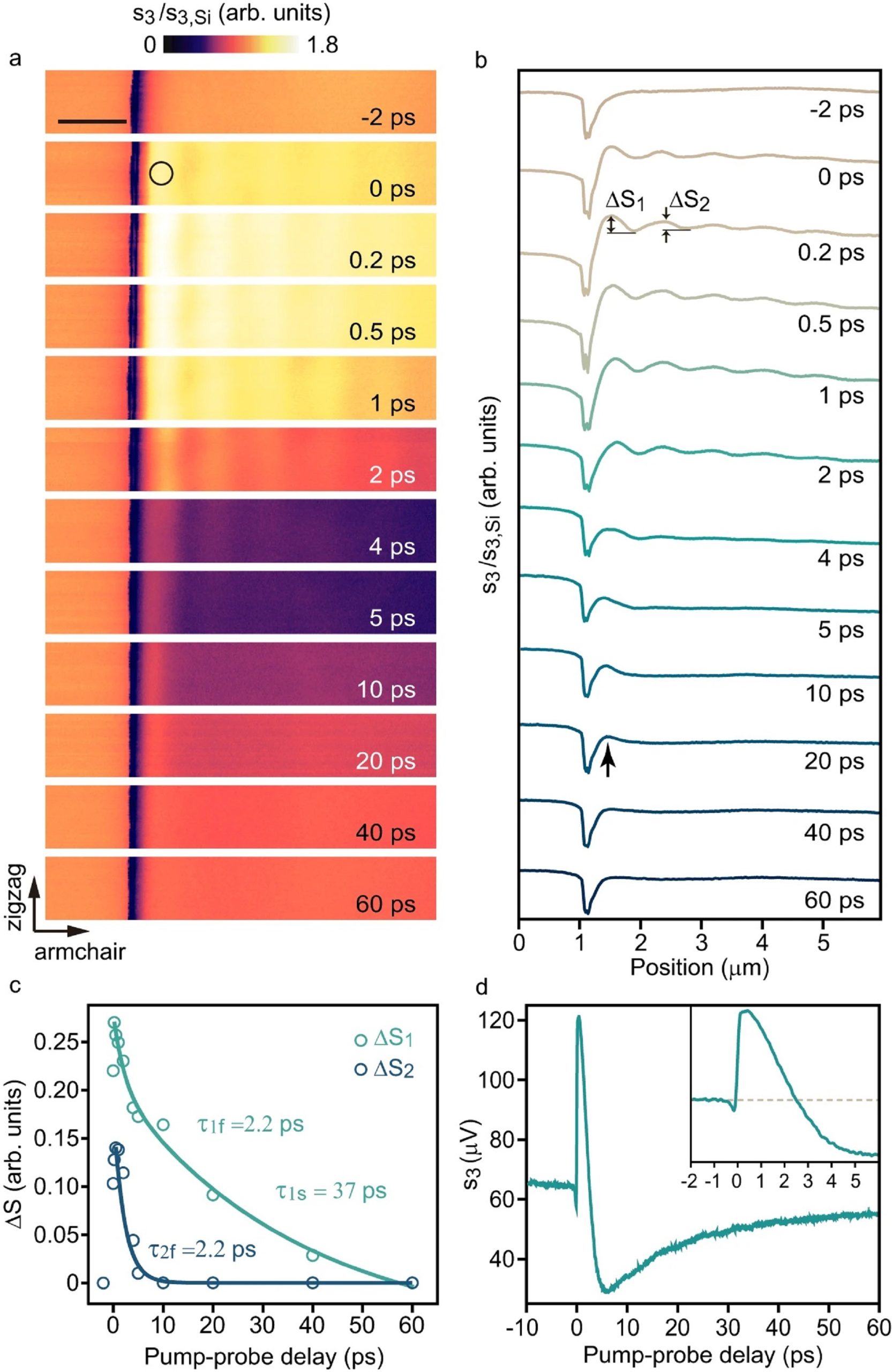
Fig. 4 from Rao Fu et al. “Manipulating hyperbolic transient plasmons in a layered semiconductor”:Dynamic analysis of the transient plasmons. a Normalized near-field amplitude s3/s3,Si of a 280-nm-thick BP slab for twelve delay times τ. Scale bar, 1 µm. b Near-field amplitude curves for the corresponding twelve different delay times τ in a. c Dynamics of the relative near-field intensity of the first (∆S1) and the second bright strip (∆S2) in b. Opened circles are the experimental data, and solid lines are bi-exponential fitting for ∆S1 and exponential fitting for ∆S2, respectively. d Dynamics of the near-field amplitude s3 from the black circle in a. The inset displays the s3 at τ = −2 to 6 ps, and the dashed line marks the s3 level of the pristine state. NanoWorld® ARROW-NCPt AFM probes with a Pt/Ir coating were used for the characterization with ultrafast nanoscopy. The pump and probe pulses were spatially overlapped on the Pt/Ir coated Arrow probe through a parabolic mirror of a commercial scattering-type scanning near-field optical microscope.
Fig. 4 from Rao Fu et al. “Manipulating hyperbolic transient plasmons in a layered semiconductor”:
Dynamic analysis of the transient plasmons.
a Normalized near-field amplitude s3/s3,Si of a 280-nm-thick BP slab for twelve delay times τ. Scale bar, 1 µm. b Near-field amplitude curves for the corresponding twelve different delay times τ in a. c Dynamics of the relative near-field intensity of the first (∆S1) and the second bright strip (∆S2) in b. Opened circles are the experimental data, and solid lines are bi-exponential fitting for ∆S1 and exponential fitting for ∆S2, respectively. d Dynamics of the near-field amplitude s3 from the black circle in a. The inset displays the s3 at τ = −2 to 6 ps, and the dashed line marks the s3 level of the pristine state.

*Rao Fu, Yusong Qu, Mengfei Xue, Xinghui Liu, Shengyao Chen, Yongqian Zhao, Runkun Chen, Boxuan Li, Hongming Weng, Qian Liu, Qing Dai and Jianing Chen
Manipulating hyperbolic transient plasmons in a layered semiconductor

Nature Communications volume 15, Article number: 709 (2024)
DOI: https://doi.org/10.1038/s41467-024-44971-3

Please follow this external link to read the full article: https://rdcu.be/dBD85

The article “Manipulating hyperbolic transient plasmons in a layered semiconductor” by Rao Fu, Yusong Qu, Mengfei Xue, Xinghui Liu, Shengyao Chen, Yongqian Zhao, Runkun Chen, Boxuan Li, Hongming Weng, Qian Liu, Qing Dai and Jianing Chen is licensed under a Creative Commons Attribution 4.0 International License, which permits use, sharing, adaptation, distribution and reproduction in any medium or format, as long as you give appropriate credit to the original author(s) and the source, provide a link to the Creative Commons license, and indicate if changes were made. The images or other third-party material in this article are included in the article’s Creative Commons license, unless indicated otherwise in a credit line to the material. If material is not included in the article’s Creative Commons license and your intended use is not permitted by statutory regulation or exceeds the permitted use, you will need to obtain permission directly from the copyright holder. To view a copy of this license, visit https://creativecommons.org/licenses/by/4.0/.

Electrochemically Synthesized Poly(3-hexylthiophene) Nanowires as Photosensitive Neuronal Interfaces

Poly(3-hexylthiophene) (P3HT), a hole-conducting polymer, generates a lot of interest especially because of its excellent optoelectronic properties (such as good electrical conductivity and high extinction coefficient) and good processability, which make this polymer an excellent choice for building organic optoelectronic devices (e.g., organic solar cells). *

P3HT films and nanoparticles have also been used to restore the photosensitivity of retinal neurons. *

For their article “Electrochemically Synthesized Poly(3-hexylthiophene) Nanowires as Photosensitive Neuronal Interfaces” Szilveszter Gáspár, Tiziana Ravasenga, Raluca-Elena Munteanu, Sorin David, Fabio Benfenati, and Elisabetta Colombo investigated the template-assisted electrochemical synthesis of P3HT nanowires doped with tetrabutylammonium hexafluorophosphate (TBAHFP) and their biocompatibility with primary neurons. *

They were able to show that template-assisted electrochemical synthesis can relatively easily turn 3-hexylthiophene (3HT) into longer (e.g., 17 ± 3 µm) or shorter (e.g., 1.5 ± 0.4 µm) P3HT nanowires with an average diameter of 196 ± 55 nm (determined by the used template) and that the nanowires produce measurable photocurrents following illumination. *

The fact that template-assisted electrochemical synthesis combines polymerization, doping, and polymer nanostructuring into one, relatively simple step is the most important advantage of this method. The possibility of easily tuning the length of the produced nanowires represents another important advantage. *

The authors were also able to demonstrate that primary cortical neurons can be grown onto P3HT nanowires drop-casted on a glass substrate without relevant changes in their viability and electrophysiological properties, indicating that P3HT nanowires obtained by template-assisted electrochemical synthesis represent a promising neuronal interface for photostimulation. *

Szilveszter Gáspár  et al. proved the biocompability of the obtained P3HT nanowires upon incubation for different periods with primary neuronal cultures. They demonstrated that their presence does not affect the membrane properties of the neurons or the excitability of the neurons as evaluated by patch-clamp experiments. These results show the potential of the described synthesis methodology to fabricate injectable P3HT-based photosensitive nanowires with high biocompatibility, ultimately paving the way for their exploitation for neuronal photostimulation. *

Atomic Force Microscopy (AFM) was used to characterize P3HT nanowires drop-casted onto glass coverslips. *

The Atomic Force Microscopy images were obtained in air and in intermittent contact-mode using line rates as slow as 0.2 Hz and NanoWorld Pointprobe® NCSTR silicon soft-tapping AFM probes (typical values: resonant frequency 160 kHz, force constant 7.2 N m). The ratio between the set-point amplitude and the free amplitude of the AFM cantilever was set to 0.5–0.6. The obtained AFM images were used to determine both the lengths and the diameters of the nanowires. *

Figure 3 from “Electrochemically Synthesized Poly(3-hexylthiophene) Nanowires as Photosensitive Neuronal Interfaces” by Szilveszter Gáspár et al.: AFM images of “long” P3HT nanowires (A) and of “short” P3HT nanowires (B). NanoWorld Pointprobe NCSTR soft-tapping mode probes were used.
Figure 3 from “Electrochemically Synthesized Poly(3-hexylthiophene) Nanowires as Photosensitive Neuronal Interfaces” by Szilveszter Gáspár et al.:
AFM images of “long” P3HT nanowires (A) and of “short” P3HT nanowires (B).

*Szilveszter Gáspár, Tiziana Ravasenga, Raluca-Elena Munteanu, Sorin David, Fabio Benfenati, and Elisabetta Colombo
Electrochemically Synthesized Poly(3-hexylthiophene) Nanowires as Photosensitive Neuronal Interfaces
Materials 2021, 14(16), 4761, Special Issue Advanced Designs of Materials, Devices and Techniques for Biosensing
DOI: https://doi.org/10.3390/ma14164761 (please follow this external link to read the full article.)

Open Access The article “Electrochemically Synthesized Poly(3-hexylthiophene) Nanowires as Photosensitive Neuronal Interfaces” by Szilveszter Gáspár, Tiziana Ravasenga, Raluca-Elena Munteanu, Sorin David, Fabio Benfenati, and Elisabetta Colombo is licensed under a Creative Commons Attribution 4.0 International License, which permits use, sharing, adaptation, distribution and reproduction in any medium or format, as long as you give appropriate credit to the original author(s) and the source, provide a link to the Creative Commons license, and indicate if changes were made. The images or other third party material in this article are included in the article’s Creative Commons license, unless indicated otherwise in a credit line to the material. If material is not included in the article’s Creative Commons license and your intended use is not permitted by statutory regulation or exceeds the permitted use, you will need to obtain permission directly from the copyright holder. To view a copy of this license, visit http://creativecommons.org/licenses/by/4.0/.