Organic-inorganic halide perovskites are materials of high interest for the development of solar cells.
Learning more about the relationship between the electrical properties and the chemical compositions of perovskite at the nanoscale can help to understand how the interrelations of both can affect device performance and contribute to an understanding on how to best design perovskite active layer structures.*
For the article “Quantification of electron accumulation at grain boundaries in perovskite polycrystalline films by correlative infrared-spectroscopic nanoimaging and Kelvin probe force microscopy” Ting-Xiao Qin, En-Ming You, Mao-Xin Zhang, Peng Zheng, Xiao-Feng Huang, Song-Yuan Ding, Bing-Wei Mao and Zhong-Qun Tian used correlative infrared-spectroscopic nanoimaging ( IR-spectroscopy ) by scattering-type scanning near-field optical microscopy ( s-SNOM ) and Kelvin probe force microscopy ( KPFM ) to contribute to the discussion whether nanometer-sized grain boundaries (GBs) in polycrystalline perovskite films play a positive or negative role in solar cell performance.*
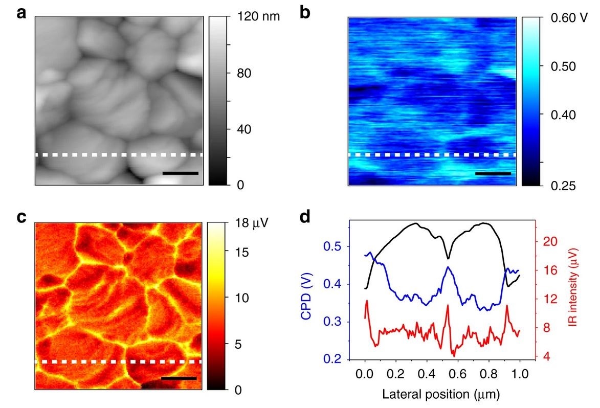
The integrated KPFM and s-SNOM measurements were performed by the authors to acquire the surface potential and infrared near-field image simultaneously through a single-pass scan and thereby learn more about the relationships between the electrical properties and spectral information at the grain boundaries of the investigated material ( polycrystalline CH3NH3Pbl3 perovskite films ).*
The results of the correlated s-SNOM and KPFM imaging presented in the article show that the electron accumulations are enhanced at the grain boundaries (GBs) of the investigated polycrystalline perovskite film, particularly under light illumination which would assist in electron-hole separation and therefore would be a positive influence on the performance of the solar cell.*
NanoWorld conductive platinum-iridium coated Arrow AFM probes ( Arrow-NCPt ) were used to perform the s-SNOM IR imaging.

Correlative KPFM and s-SNOM nanoimaging on perovskite.
a AFM topography (1 μm × 1 μm); b Contact potential difference (CPD); and c simultaneously acquired infrared near-field image; d one-dimensional line profiles of the topography, CPD and infrared near-field amplitude along the white dashed lines marked in a–c. The scale bars are 200 nm.
*Ting-Xiao Qin, En-Ming You, Mao-Xin Zhang, Peng Zheng, Xiao-Feng Huang, Song-Yuan Ding, Bing-Wei Mao and Zhong-Qun Tian
Quantification of electron accumulation at grain boundaries in perovskite polycrystalline films by correlative infrared-spectroscopic nanoimaging and Kelvin probe force microscopy
Light: Science & Applications volume 10, Article number: 84 (2021)
DOI: https://doi.org/10.1038/s41377-021-00524-7
Please follow the external link to read the whole article: https://rdcu.be/clg7f
Open Access : The article “Quantification of electron accumulation at grain boundaries in perovskite polycrystalline films by correlative infrared-spectroscopic nanoimaging and Kelvin probe force microscopy” by Ting-Xiao Qin, En-Ming You, Mao-Xin Zhang, Peng Zheng, Xiao-Feng Huang, Song-Yuan Ding, Bing-Wei Mao and Zhong-Qun Tian is licensed under a Creative Commons Attribution 4.0 International License, which permits use, sharing, adaptation, distribution and reproduction in any medium or format, as long as you give appropriate credit to the original author(s) and the source, provide a link to the Creative Commons license, and indicate if changes were made. The images or other third party material in this article are included in the article’s Creative Commons license, unless indicated otherwise in a credit line to the material. If material is not included in the article’s Creative Commons license and your intended use is not permitted by statutory regulation or exceeds the permitted use, you will need to obtain permission directly from the copyright holder. To view a copy of this license, visit https://creativecommons.org/licenses/by/4.0/.

![Figure 2 from "Boron nitride nanoresonators for phonon-enhanced molecular vibrational spectroscopy at the strong coupling limit": Far- and near-field spectroscopic characterization of h-BN ribbon arrays. (a) Sketch of the transmission spectroscopy experiment. Incoming light at normal incidence is polarized perpendicular to the ribbons to excite the HPhP resonance. (b) Transmission spectrum normalized to the bare substrate spectrum, T/T0, for a 20 × 20 μm2 h-BN ribbon array. Ribbon width w=158 nm, ribbon period D=400 nm and ribbon height h=40 nm. (c) Sketch of the nano-FTIR spectroscopy experiment. The near-field probing tip is scanned across (y-direction) the h-BN ribbon in 20-nm steps, as indicated by the dashed blue line. Near-field spectra are recorded as a function of the tip position (the detector signal is demodulated at the third harmonic of the tip tapping frequency, yielding s3(y, ω), as explained in the Materials and methods section). (d) Lower panel: Spectral line scan s3(y, ω), where each horizontal line corresponds to a spectrum recorded at a fixed y-position (vertical axis). Upper panel: Illustration of the real part of the z-component of the electric field (Re[Ez]) profile across the ribbon at the resonance frequency observed in the nano-FTIR spectra (lower panel). The AFM tip used was a NanoWorld Arrow-NCPT](https://dhipgo7nn2tea.cloudfront.net/wp-content/uploads/2018/09/24110501/Figure-2-from-Boron-nitride-nanoresonators-for-phonon-enhanced-molecular-vibrational-spectroscopy-at-the-strong-coupling-limit.jpg)