Physical properties of the polycrystalline materials are mostly determined by their microstructure. As the crystallization process can determine the microstructure, the nucleation, and growth can also control whether the materials will be resulted in single crystalline or polycrystalline. Along with the morphological changes, anisotropic properties of the materials can also be controlled. *
As a result, preferential orientation with advanced optoelectronic properties can enhance the photovoltaic devices’ performance. *
Although incorporation of additives is one of the most studied methods to stabilize the photoactive α-phase of formamidinium lead tri-iodide (α-FAPbI3), no studies focus on how the additives affect the crystallization kinetics. *
In the article “Kinetic-Controlled Crystallization of α-FAPbI3 Inducing Preferred Crystallographic Orientation Enhances Photovoltaic Performance” along with the role of methylammonium chloride (MACl) as a “stabilizer” in the formation of α-FAPbI3, Sooeun Shin, Seongrok Seo, Seonghwa Jeong, Anir S. Sharbirin, Jeongyong Kim, Hyungju Ahn, Nam-Gyu Park and Hyunjung Shin point out the additional role as a “controller” in the crystallization kinetics. *
With microscopic observations, for example, electron backscatter diffraction and selected area electron diffraction, it is examined that higher concentration of MACl induces slower crystallization kinetics, resulting in larger grain size and [100] preferred orientation. *
Optoelectronic properties of [100] preferentially oriented grains with less non-radiative recombination, a longer lifetime of charge carriers, and lower photocurrent deviations in between each grain induce higher short-circuit current density (Jsc) and fill factor. *
Resulting MACl40 mol% attains the highest power conversion efficiency (PCE) of 24.1%.
The results provide observations of a direct correlation between the crystallographic orientation and device performance as it highlights the importance of crystallization kinetics resulting in desirable microstructures for device engineering. *
The electrical characterizations with atomic force microscopy (AFM) and conductive atomic force microscopy ( C-AFM) were done to measure the local conductance of FAPbI3 films. All measurements were performed under illumination (green LED) with a 1.3 V bias using a Pt-coated C-AFM probe (NanoWorld PlatinumIridium coated Pointprobe® CONTPt ). FTO was used for the conductive substrates. *
Conductive atomic force microscopy (C-AFM) indicated much more homogeneous photocurrent generation along the surface of (100) preferentially oriented layers. *
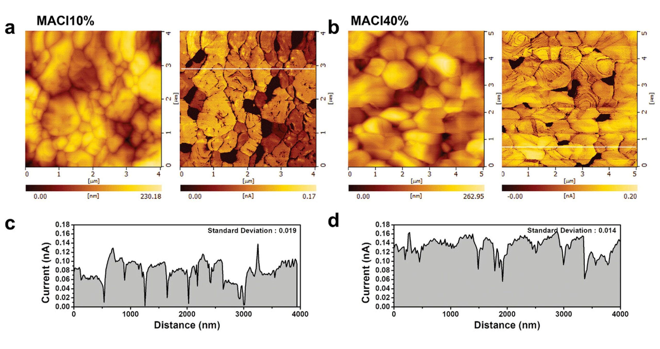
Electrical properties of (100)-oriented α-FAPbI3 thin films. a,b) Surface topography and photocurrent measurement by C-AFM of MACl10% and MACl40%. Measurements were taken under illumination (green LED) with a 1.3 V bias. Current images indicate that photocurrents were induced grain by grain, as each grain showed a distinct photocurrent. The photocurrent deviation for each grain is larger in MACl10% than in MACl40%, which shows a similar photocurrent grain by grain. c,d) Current line profile extracted from the current image (a and b). The standard deviation calculated from the magnitude of the photocurrent in each grain is displayed in the inset (0.019 and 0.014 nA for MACl10% and MACl40%, respectively). A low photocurrent was exhibited at the grain boundaries in both MACl10% and MACl40%. The dark areas measured within the current images are most likely distributed between grain edges. This may be caused by the formation of PbI2 or the loss of contact between the grain and the conducting substrate.
*Sooeun Shin, Seongrok Seo, Seonghwa Jeong, Anir S. Sharbirin, Jeongyong Kim, Hyungju Ahn, Nam-Gyu Park and Hyunjung Shin
Kinetic-Controlled Crystallization of α-FAPbI3 Inducing Preferred Crystallographic Orientation Enhances Photovoltaic Performance
Advanced Science, Volume 10, Issue 14, May 17, 2023, 2300798
DOI: https://doi.org/10.1002/advs.202300798
Open Access The article “Kinetic-Controlled Crystallization of α-FAPbI3 Inducing Preferred Crystallographic Orientation Enhances Photovoltaic Performance” Sooeun Shin, Seongrok Seo, Seonghwa Jeong, Anir S. Sharbirin, Jeongyong Kim, Hyungju Ahn, Nam-Gyu Park and Hyunjung Shin is licensed under a Creative Commons Attribution 4.0 International License, which permits use, sharing, adaptation, distribution and reproduction in any medium or format, as long as you give appropriate credit to the original author(s) and the source, provide a link to the Creative Commons license, and indicate if changes were made. The images or other third party material in this article are included in the article’s Creative Commons license, unless indicated otherwise in a credit line to the material. If material is not included in the article’s Creative Commons license and your intended use is not permitted by statutory regulation or exceeds the permitted use, you will need to obtain permission directly from the copyright holder. To view a copy of this license, visit http://creativecommons.org/licenses/by/4.0/.