The ability to maximize the range of exciton transport while minimizing energy loss has significant implications for the design of future nanoscale light harvesting, optoelectronic, and sensing applications. *
One method of achieving this would be to densely pack dyes into strongly coupled aggregates such that excitations can be coherently delocalized through the partial or full length of the aggregate. *
Coherently coupled aggregates enable exciton migration over discreet spatial distances with near unitary quantum efficiency. As a result, controlled dye aggregation has long been studied by chemists as a method of tuning the photonic and physical properties of the dyes and pigments in light harvesting devices. An example of this coherent coupling phenomenon can be observed in the cyanine dye family and specifically the prototypical example, pseudoisocyanine (PIC) dye. *
In the article «Structural and optical variation of pseudoisocyanine aggregates nucleated on DNA substrates” Matthew Chiriboga, Christopher M Green, Divita Mathur, David A Hastman, Joseph S Melinger, Remi Veneziano, Igor L Medintz and Sebastián A Díaz show that DNA-nucleated PIC aggregates have properties which correlate to different molecular structures and are directed by changing the DNA scaffold. *
To achieve this, they formed PIC aggregates through heterogeneous nucleation by mixing dissolved PIC dye with various DNA nanostructures ranging from a rigid DX-tile to more flexible DNA duplex (dsDNA) or single strand DNA oligonucleotide (ssDNA). *
Although the aggregates Matthew Chiriboga et al formed required elevated excess of PIC dye relative to previously reported J-bits, they exhibited sharper and brighter fluorescence peaks as well as longer Ncoh. *
Therefore, the authors refer to aggregates formed by this approach as super aggregate (SA) in their article, though they note SA formed with different DNA substrates result in unique properties. *
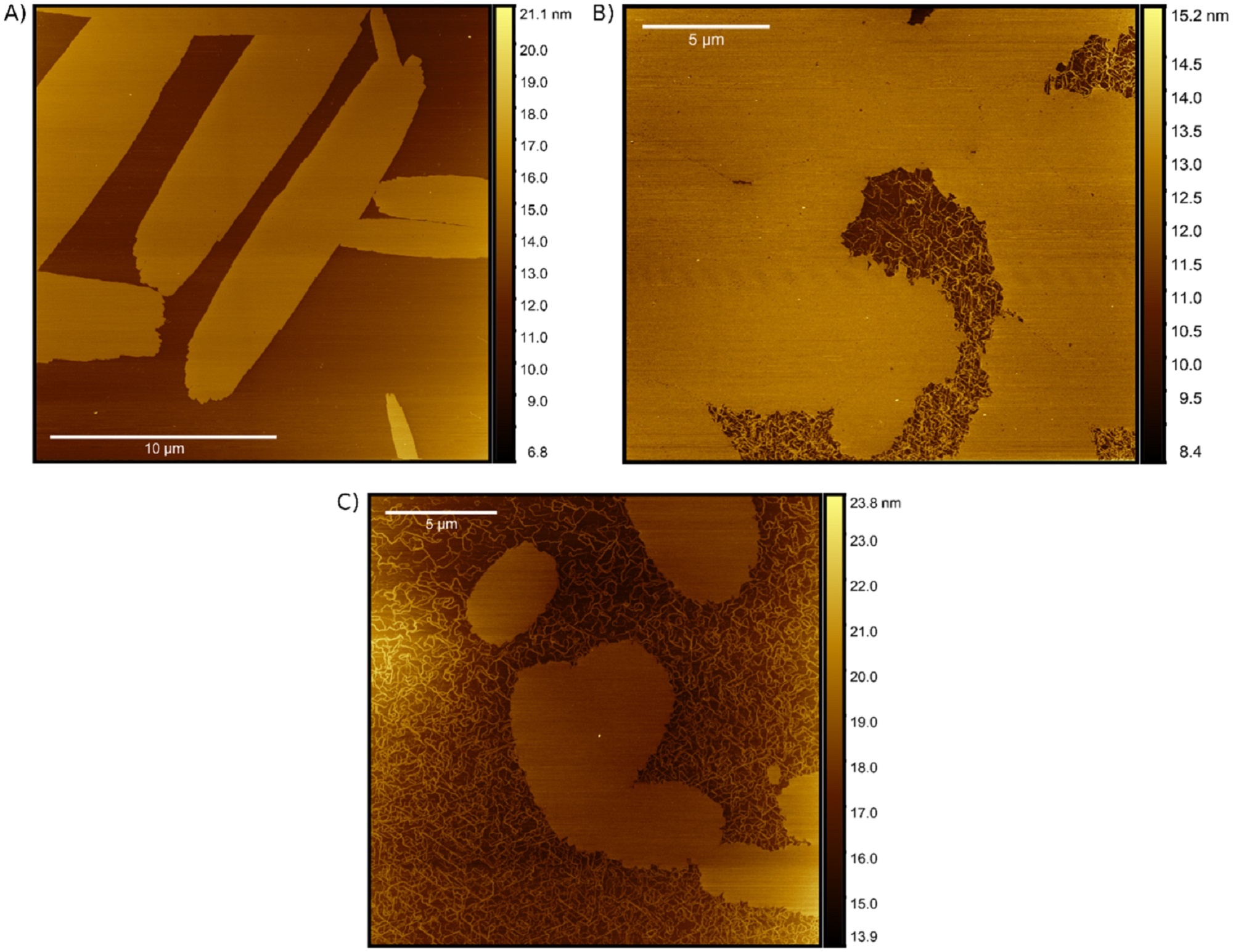
Complementary circular dichroism (CD) and atomic force microscopy (AFM) characterizations were used to analyze the SA and both indicated distinctions in the way each substrate and subsequent dye aggregate incorporates the individual PIC molecules. *
To achieve high resolution imaging of nucleic acid nanostructures, the DNA is often deposited onto a mica substrate, where mica electrostatically binds the DNA. Once deposited onto the mica, the imaging can be done in a hydrated environment as there is no additional required dehydration or staining of the DNA, a particularly convenient advantage of AFM. *
The AFM imaging was performed under AC fast imaging mode (liquid) with NanoWorld Ultra-Short Cantilevers (USC) for Fast/High-Speed AFM of the USC-F0.3-k0.3 AFM probe type.*
On a segment of freshly cleaved mica mounted to a magnetic puck, 15 μl of PIC-DANN solution was deposited immediately before measurement. A 25 μl droplet of imaging buffer was deposited on the AFM tip, then the AFM tip mount was lowered into the sample buffer to create a liquid ‘chamber’ for imaging. *
When introducing various DNA scaffolds for SA formation and subsequent AFM imaging, Matthew Chiriboga et al. observed significant changes in the aggregates structure. *
The AFM imaging highlighted the stark differences in aggregate formation resulting from the DNA substrates. *
To the author’s knowledge this is the first visualization of DNA-based PIC aggregates. Results from the field have been pointing towards fiber-like or nanotube-like networks of polymerized PIC as a structural model for aggregates suspended in solution. *
On the other hand, other AFM studies demonstrate that PIC aggregates formed on mica substrates adopt a leafy island morphology. *
Interestingly, Matthew Chiriboga et al. observe evidence of both PIC fibers as well as leafy islands that exhibit distinct growth patterns, again depending on the DNA substrate. *
Although this work contributes to the growing body of evidence that solution-based PIC aggregates form fibrous networks structures, the AFM measurements presented in the article highlight the multiplicity of PIC aggregation modes when introduced to DNA scaffolds. *
The results presented in the research article suggest modification of the DNA substrate results in significant changes to how the DNA and companion dye molecules are integrated into larger form PIC aggregates. *
Bearing in mind that the broader motivation for studying DNA based PIC aggregates is to integrate strongly coupled dyes onto modular DNA structural units, PIC SAs should be given due consideration as a versatile option. *
In fact, similar work is being done with other cyanine dyes where DNA template modification is used to switch between quenching and energy transfer. *
Ultimately this could be a path for the PIC SA and one which possibly leads towards applications in optical microcavities for quantum electrodynamical devices and optical switching, molecular plasmonics, biosensors, and light-harvesting arrays. *

AFM visualization of SA formations. AFM visualizations of PIC aggregates formed in the (A) AT, (B) dsDNA, and (C) ssDNA nanostructures. Each of the samples was formed immediately before measurement by mixing 160 μM PIC dye with 500 nM DNA normalized to the dye-labeled strand concentration (i.e. 320-fold excess).
*Matthew Chiriboga, Christopher M Green, Divita Mathur, David A Hastman, Joseph S Melinger, Remi Veneziano, Igor L Medintz and Sebastián A Díaz
Structural and optical variation of pseudoisocyanine aggregates nucleated on DNA substrates
Methods and Applications in Fluorescence (2023) 11 014003
DOI: https://doi.org/10.1088/2050-6120/acb2b4
The article “Active self-assembly of piezoelectric biomolecular films via synergistic nanoconfinement and in-situ poling” by Matthew Chiriboga, Christopher M Green, Divita Mathur, David A Hastman, Joseph S Melinger, Remi Veneziano, Igor L Medintz and Sebastián A Díaz is licensed under a Creative Commons Attribution 4.0 International License, which permits use, sharing, adaptation, distribution and reproduction in any medium or format, as long as you give appropriate credit to the original author(s) and the source, provide a link to the Creative Commons license, and indicate if changes were made. The images or other third-party material in this article are included in the article’s Creative Commons license, unless indicated otherwise in a credit line to the material. If material is not included in the article’s Creative Commons license and your intended use is not permitted by statutory regulation or exceeds the permitted use, you will need to obtain permission directly from the copyright holder. To view a copy of this license, visit https://creativecommons.org/licenses/by/4.0/.


