Have you every wondered how carbon dating in the AFM tip world works?

Have you every wondered how carbon dating in the AFM tip world works?
In the article cited below Katherine Atamanuk, Justin Luria and Bryan D. Huey present “a new approach for directly mapping VOC (open-circuit voltage) with nanoscale resolution, requiring a single, standard-speed AFM scan. This leverages the concept of the proportional-integral-derivative (PID) feedback loop that underpins nearly all AFM topography imaging.”*
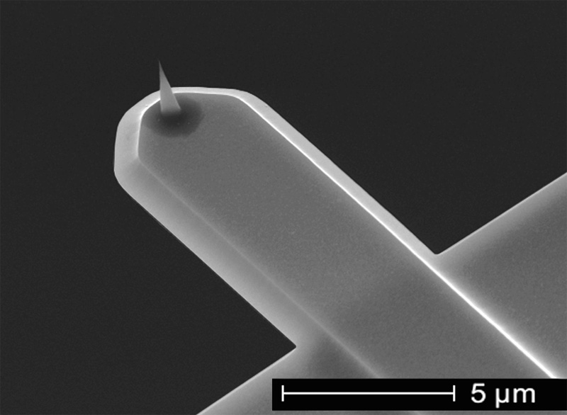
NanoWorld™ Pointprobe® CDT-NCHR conductive diamond coated silicon AFM probes were used in the described CT-AFM experiment.
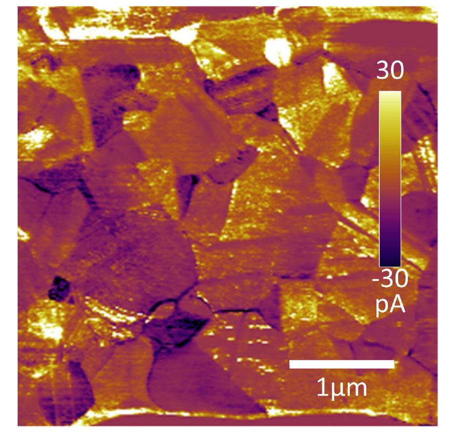
“Cadmium Telluride (CdTe) is an inexpensive thin-film photovoltaic with ca. 5% of the 2017 global market share for solar cells. To optimize the efficiency and reliability of these, or any electronic devices, a thorough understanding of their composition, microstructure, and performance is necessary as a function of device design, processing, and in-service conditions. Atomic force microscopy (AFM) has been a valuable tool for such characterization, especially of materials properties and device performance at the nanoscale. In the case of thin-film solar cells, local photovoltaic (PV) properties such as the open-circuit voltage, photocurrent, and work function have been demonstrated to vary by an order of magnitude, or more, within tens of nanometers […] Recently, property mapping with high spatial resolution by AFM has been further combined with the ability to serially mill a surface, in order to reveal underlying surface structures and uniquely develop three-dimensional (3D) nanoscale property maps. The most notable examples are based on pure current detection with the AFM to resolve conduction pathways in filamentary semiconducting devices and interconnects […], and tomographic AFM of photocurrents in polycrystalline solar cells during in situ illumination […].”*
*Katherine Atamanuk, Justin Luria, Bryan D. Huey
Direct AFM-based nanoscale mapping and tomography of open-circuit voltages for photovoltaics
Beilstein Journal of Nanotechnology 2018, 9, 1802–1808.
doi: 10.3762/bjnano.9.171
The article cited above is part of the Thematic Series “Scanning probe microscopy for energy-related materials”.
Please follow this external link for the full article: https://www.beilstein-journals.org/bjnano/articles/9/171
The article “Direct AFM-based nanoscale mapping and tomography of open-circuit voltages for photovoltaics” by Atamanuk et. al is an Open Access article under the terms of the Creative Commons Attribution License (http://creativecommons.org/licenses/by/4.0), which permits unrestricted use, distribution, and reproduction in any medium, provided the original work is properly cited.
If you would like to see what has been going on in the last few years in the field of high speed AFM then have a look at: http://www.highspeedscanning.com/hs-afm-references.html
We know that this list is far from complete so if you have used one of our USC tips in the research for your publication and your article isn’t listed yet then please let us know.